Hi Stocker,
You are surprised by the inefficiency of bipolar pure class-A, but the sound is clean without complexity.
Cheers ......... Graham.
You are surprised by the inefficiency of bipolar pure class-A, but the sound is clean without complexity.
Cheers ......... Graham.
Hi Graham,
thanks
Sorry if I miss a boat, but this aabb stage is also pure current drive, isn't it?Graham Maynard said:I believe my mistake to date has been applying current drive instead of voltage drive in my attempt to use the low distortion JLH output arrangement.
I tried that already. IIRC I mentioned that adding small CCS to BD139 emitter made very little difference. As I see it, this makes no difference to the output stage, and only if splitter itself benefits from more current through it, it might be helpful. But in my sims, the change in distortion was to negative impact..Suggestion;- add another transistor to the CCS so that you double up on Q2, and use this to sink some standing current through the BD139.
I tried that first. That by itself already increased thd, and added emitter resistor only made it worse. Equal boostrap resistors simulates best results in my case. I'm still missing something I'm afraid.Adding the driver emitter resistor is increasing distortion because your bootstrapped collector resistors have equal value. The upper one is better being much lower in the JLH output stage.
But is it just that? I thought it has to do with reducing impact of input BJT capacitance. This affects propagation delay as I see it, and thus reduces NFB lag. I thought this is the more important factor here. It tightens up the NFB correction.Lower resistance at the input transistor emitter reduces thd by increasing the ratio between emitter resistance and R7/Q7 resistance/impedance; ie. increasing stage gain.
What do you mean badly balanced? As I see it, its as balanced as possible. Please elaborate, this is important moment I don't want to miss.The FFT is not bad considering how badly balanced your investigative circuit is.
When I'll get to making power, this aabb will be the one I'll sure try.And the big question; are you adventurous enough to try it in real life ?
thanks
Hi Wimms,
The AABB configuration can be voltage driven too; different emitter resistor selection may be necessary.
You can get different THD results at different AABB bias levels, so it might not be only the driver resistors that are causing your observed measurements, you might simultaneously be affecting the bias.
My view of the JLH ouput stage is that it is the output devices that contribute most to propagation delay, unless the first and second transistors are run at miniscule current.
To check for balance place Ammeters in series with the combined AABB 'collector' leads. Run the circuit with both high and low level inputs.
Cheers ........... Graham.
Hi Graham !
I have a few questions which I hope You`ll answer.
1. Would it be a good idea to just add the two class-B transistors to a JLH or your 25W ?
2. I wonder why You have put a 47K resistor to ground from the base of the phase-splitter ? I believe that one of the benefits of the current-mirror is the high output-impedance which results in equal output-impedance from the phase-splitter ( as its input has no ground reference ).
3. Which is the best sounding JLH-variant in your opinion?
I love the sound from a good JLH.
I wish You good health !
Thorsten
Graham Maynard said:Hi Stocker,
You are surprised by the inefficiency of bipolar pure class-A, but the sound is clean without complexity.
Cheers ......... Graham.
The sound is not in question nor was I surprised at the efficiency (it's quite high actually)
I was surprised that I caught it! I am learning still.
Hi Thorsten,
Adding class-B only, makes for too much discongruity.
One of the problems of the JLH is that the lower output transistor can receive input stage base current through the splitter transistor. I tried the 47k resistor for an approx 1mA max splitter base current, but this was also the emitter feed to the first stage follower.
I have built many variations, and prefer my 25W with the differential and mirror for its better damping factor, detail and much improved dynamic and bias stabilities.
_________________________________________________________
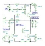
I have attached my next test bed for the class-AABB. Unfortunately I am not feeling good at the moment and it is likely that I will not be able to construct for some time.
Here I have used two separate 2SC3241 drivers with differential drive so that the currents cannot be other than always opposing, with the output stage never dropping out of class-A whilst maintaining good balance and impedance dip driving capabilities.
The diode can temperature compensate for increased quiescent current with long term high output.
Without a VAS like driver, the zero offset of this circuit is tiny.
The 75k and 69p (47+22) components are to approx equalise the internal characteristics between upper and lower current cascodes.
I have assumed 50ohm pre-amp output with 200pf cable impedance. The 10k input resistor could be changed to 1k for 600 ohm input.
This does not have super low distortion, but it does have very low internal reactivity and high power transient capability.
Cheers ........... Graham.
Adding class-B only, makes for too much discongruity.
One of the problems of the JLH is that the lower output transistor can receive input stage base current through the splitter transistor. I tried the 47k resistor for an approx 1mA max splitter base current, but this was also the emitter feed to the first stage follower.
I have built many variations, and prefer my 25W with the differential and mirror for its better damping factor, detail and much improved dynamic and bias stabilities.
_________________________________________________________
I have attached my next test bed for the class-AABB. Unfortunately I am not feeling good at the moment and it is likely that I will not be able to construct for some time.
Here I have used two separate 2SC3241 drivers with differential drive so that the currents cannot be other than always opposing, with the output stage never dropping out of class-A whilst maintaining good balance and impedance dip driving capabilities.
The diode can temperature compensate for increased quiescent current with long term high output.
Without a VAS like driver, the zero offset of this circuit is tiny.
The 75k and 69p (47+22) components are to approx equalise the internal characteristics between upper and lower current cascodes.
I have assumed 50ohm pre-amp output with 200pf cable impedance. The 10k input resistor could be changed to 1k for 600 ohm input.
This does not have super low distortion, but it does have very low internal reactivity and high power transient capability.
Cheers ........... Graham.
Attachments
Hi Graham !
Your "gem" looks a lot like an amp I build a few years ago. Exept that I just used Mosfets as outputs. Just a dif-pair ( Mos´s too) whith folded cascodes directly driving two NPN Mosfets. It worked and sounded just fine. But the measured distortion was pretty high because I used lateral Mosfets. ( low open loop gain )
Hope You are feeling better.
Thorsten
Hi Thorsten,
Mosfets after the bootstrap class-A biased 2SC3241 buffer/driver might work well, but I am not experienced enough with these devices to be sure that additional stabilising components will not be required in order to obtain a high power output.
I had not actually checked this circuit for open loop characteristics other than 0dB gain stability, this because I had been primarily studying its reverse (dynamic loudspeaker controlling) behaviour.
This latest AABB circuit has an open loop gain of approx 75dB with -3db @ circa 100kHz, and a nicely clean non-nfb feedback first cycle sinewave distortion of 0.6% at 1kHz - 50W - 8 ohms.
( N.B. The compensating R and C components must be given different values for different open/closed loop gains because they are output terminal driven. )
Cheers ........... Graham.
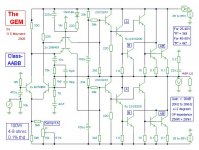
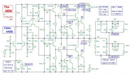
I called the output stage in this string 'Class-AABB' because all three 'A', 'B' plus 'C' modes of operation are utilised on a per cycle basis.
There is now available an 'AABB' upgrade to the PrimaLuna 'ProLogue One' stereo valve amplifier. Here though these initials stand for Adaptive AutoBias Board, which dynamically modifies the fixed bias to each pair of class-AB EL34 output valves in order to minimise momentary elevated levels of crossover distortion at large amplitude and low frequency.
Hi Thorsten,
You mentioned your amplifier of a few years ago sounding just fine, but that you measured the distortion and found it pretty high.
I wonder if I could trouble you to ask this question;- did the measurement figures influence your conclusions about the amplifier, or were you actually able to hear something specific that put you off investigating further developments ?
I look forwards to hearing of your 25W findings too.
There are many who backed off from constructing this amplifier. They contacted me to state that it oscillates, but this was on their simulators, which they believed !!!
However, I have run this circuit in real life, and yes it could be made to oscillate with inappropriate wiring, but the real crux of the matter is that simulator software does not facilitate checking circuits where the low level (input) transistors run at room temperature whilst outputs run with increased gain but reduced bandwidth at much higher (class-A) dissipations !
Cheers ............. Graham.
Just realised I wrote A + B + C instead of A + AB + B.
If you did not work out what I really meant to write, then please understand that my head injury has recently been much more of a problem, and in many more ways than this, to me.
Cheers ............. Graham.
If you did not work out what I really meant to write, then please understand that my head injury has recently been much more of a problem, and in many more ways than this, to me.
Cheers ............. Graham.
Hi Graham !
I think I got what You meant. I only build one channel just to see if the idea would work. I measured it and listened to it and decided that If I should build another channel I would use industrial mosfets, because they have higher gm and higher Vgs, which both would give higher open loop gain. But that would require some thermal compensation. My decision was mainly based on measurements.
The idea was to make a two stage amp with only N-channel fets and to utilize the inherrent nonlinearity of the mosfets to make some kind of efficient non-switching class-A. The same as in Susans Zeus.
I now see that the JLH and Your new amps work in a similar way by driving the high and low side independent. I think it is an interesting path. I`ll try to attach a schematic. The component and values are not correct.
Take care.
Thorsten
Attachments

Hi Thorsten,
Thanks for offering your original idea.
If your I1 and I2 sources were changed to (inherently stailising) resistors tied to the V4 +ve rail, then a ground to rail resistor plus diode base bias for Q3/4 (like mine), with resistor bias for Q1/2, the circuit could track mains voltage/psu variations, also with the diode (think I will use a BD139 with base plus collector shorted) bolted to the heatsink or piggy back on an output device, then the standing splitter current can be made to track hot output devices.
Your peak Q3/4 current across R3/4 could also set the maximum gate voltage, and with no reverse flow possible other than via the gate resistor then I think maybe no protection would actually be necesary.
A follower buffer between your Q3 and5 also Q4 and 6should allow you to divide Q1 to Q4 standing currents by a factor of ten to improve both open loop gain and bandwidth, but this would introduce another minor hf phase shift within the closed loop.
____________________________________________________________
Regarding my JLH/AABB approach, yes, when both output halves are separately driven, the propagation delayed correction in response to back EMF that affects a predominantly conducting output half can be independently countered by both output halves without the normal corrections in drive to say a hard conducting complementary output half simultaneously affecting the common push-pull drive to its other half ... Here the lesser conducting half can still effectively correct without it being directly affected by any of the charge collection delays imposed by its deeper conducting (and normally bias chain connected) partner.
I did not set out to mimic Mosfet characteristics with my AABB output composite, but it seems to behave similarly with voltage drive. It does of course have substantially increased drive current requirements, though these are actually more correctly phase coherent, and parallel connecting for increased power is much easier. My idea was like yours - to use the oppositely acting output stage transfer characteristics to maintain class-A operation, which, as you state, Susan is doing, though she has found some devices operate in push-pull more naturally than others without NFB.
Cheers ............. Graham.
Hi All,
This is the present design state for my latest class-AABB circuit.
+/- 55V rails assumed. (BD140 will need changed)
I shall be studying it a little more before constructing; hopefully before the end of April.
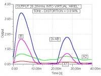
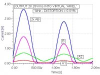
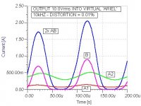
I also follow this up with some simulated current traces for one half of the output stage when sine driving the approximate circuit equivalent of an 'Ariel' loudspeaker.
This loudspeaker is not particularly load friendly to the majority of solid state amplifiers, and I illustrate how the current draw decreases after energising bass resonance at 50Hz, reduces after energising crossover circuitry plus driver at 1Khz, and increases due to composite lead loading above the crossover frequency. At 190 to 200Hz the driver loading is most direct (symmetrical plus constant) with a combined peak current draw per output stage approaching 12A @ 40V, and this for a nominally 5.3 ohm impedance loudspeaker.
Note that both of the class-AB output devices now crossover at slightly different times due to the single capacitor per half, also both of these conduction times are different to that due to class-B activity. Both Drivers operate without dropping out of class-A and thus contribute towards output control up to about 11A @ 40V when the output stage continues in a still clean class-B.
All of these waveforms start cleanly from zero without inducing any observable problems, so the response during any 'transient' first cycle is likely to be clean.
Cheers ............. Graham.
This is the present design state for my latest class-AABB circuit.
+/- 55V rails assumed. (BD140 will need changed)
I shall be studying it a little more before constructing; hopefully before the end of April.
I also follow this up with some simulated current traces for one half of the output stage when sine driving the approximate circuit equivalent of an 'Ariel' loudspeaker.
This loudspeaker is not particularly load friendly to the majority of solid state amplifiers, and I illustrate how the current draw decreases after energising bass resonance at 50Hz, reduces after energising crossover circuitry plus driver at 1Khz, and increases due to composite lead loading above the crossover frequency. At 190 to 200Hz the driver loading is most direct (symmetrical plus constant) with a combined peak current draw per output stage approaching 12A @ 40V, and this for a nominally 5.3 ohm impedance loudspeaker.
Note that both of the class-AB output devices now crossover at slightly different times due to the single capacitor per half, also both of these conduction times are different to that due to class-B activity. Both Drivers operate without dropping out of class-A and thus contribute towards output control up to about 11A @ 40V when the output stage continues in a still clean class-B.
All of these waveforms start cleanly from zero without inducing any observable problems, so the response during any 'transient' first cycle is likely to be clean.
Cheers ............. Graham.
Attachments

- Status
- Not open for further replies.
- Home
- Amplifiers
- Solid State
- Class-AABB output stage.