Hi lumanauw,
Your attachment appears to illustrate conventional Darlington cascade for high power. Whether the devices operate in class-A or AB or B would be determined by biasing circuitry you do not show.
It is very likely that this circuit does not retain any class-A operation at all. There appears to be common drive to both output halves without any form of output bias sensing; ie. the drive to one half will deliberately pull the other out of conduction.
Tubes and mosfets do require some dynamic current flow at their grid/gate electrodes. Grids are not immune to interelectrode capacitance charging requirements, though this tends to be low and near *linear* for normal operation, and is why the split load phase splitter works better in valves than with unbuffered semiconductors..
Gate charging requirements are much greater than with tubes and can be grossly non-linear with voltage.
Bipolars might be current driven but they can have considerable current/voltage variable charge retention/conduction problems too.
So its not only bipolars that suck currents - what a thought ! In old electronics days there would have been a little cartoon for this.
Hi darkfenriz,
Of course combining classes is as old as the hills, but my reason for doing this is to have higher power operation utilising two differently timed crossovers with their discontinuities almost instantly and separately smoothed by the constantly operating class-A drivers via extremely low propagation/NFB delay which disallows load back EMF driven reverse commutation.
Where a Darlington driver emitter resistor is connected to the output emitter, and that output device also has an emitter resistor, this is done as a partial bootstrap for the driver emitter load. The input impedance of the driver is thus slightly increased, but there is also a slight increase in hf phase shift beyond that with plain grounded emitter resistors. Thus, depending on the rest of the circuit, the damping factor could be slightly increased but the amplifier response slightly slowed by necessary additional stability Cs - swings and roundabouts!
There is not normally any constant class-A operation in classic solid state 'AB' circuits, though I believe P. Tharma did acheive this in one of his 1960s Mullard germanium designs. I still have his book somewhere in the roofspace.
Hi Grollins,
Sorry to hear you have so little time for your dipping.
Two things for sure about simulations, they cannot guarantee for whether an amplifier circuit will oscillate in real life, and they cannot indicate what a finished power amplifier will sound like with any particular loudspeaker system.
Hi Hans,
JCX's simulations in his above reference illustrated two unreal aspects related to computerised device activity. Most simulator users would not be aware of these and might thus might always have accepted them is if actual.
Rubbish in - rubbish out, yes - and - but, this also applies to the software packaged models themselves.
I have gained much insight by observing simulations, though from back when a friend ran them for me before I had a computer, I still cannot trust them. Nothing beats hands/ears-on, and it is not as if there are not any examples of software optimised designs that give problems in the real world either.
Hey, this class-AABB might not turn out to be good compared to others ......... Graham.
Hi Graham,
Re simulations, I agree with something you say, (model quality, rubbish in-Rubbish out etc). As DIY I only work with tubes and especially for tubes it is very difficult to find models that are accurate, I modify available models based on measurements on real circuits in order to reach a reasonable degree of accuracy as I find this to be an interesting excercise. What is maybe the most difficult to simulate correctly is unlinearities as the models of active devices often fall apart at the extremes, (very low or very high voltages/currents) and OTOH what is relatively easy to simulate is frequency gain behavior.
I have extensive experience of simulation of linear SS devices, (especially RF) from my work so I am well aware of the quality of available simulations tools and device models, in my mind it is very difficult to imagine a modern company that wouldn't use simulation. That circuits need to be built and tested and normally also corrected after being designed and simulated goes without saying but circuit simulation shortens the design process and also allows simulation of yield and performance spread.
Regards Hans
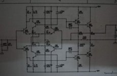
High power, with 1 ohm emitter resistors in the output stage ?
With 10 Ohm on the predriver emitters ?
Maybe Lumanauw can show the entire picture?
I had a parttime job as a system manager at a big hotel when doing time at polytech.
One day the main frame flunked and presented an extra billion dollars earnings that day.
I wished i had believed the numbers, the trade off might have made me rich.
Still, better than doing the numbers by hand every day !
"Rubbish in - rubbish out" , good enough for a motto !
Hi All,
Here are three more of my circuits.
The single ended input stage shown here works as well as the it can - - it is unbalanced, and this causes problems at larger amplitude swings.
It is though a fully tested and working alternative for those who dislike the differential input.
The second front end has also been tested, but I am not sure that the extra complexity realises any real world improvement.
This has a cascode amplified differential mirror which has an extra 20dB open loop gain/NFB potential within the first stage.
I don't know enough about Mosfets to be able to write about them, so I have placed this input stage in front of a possible Mosfet version of the JLH output stage and used a push-pull driver to set both the quiescent bias and provide missing lower transistor pull-down.
In view of my listenings to the bipolar JLH with balanced output drive and fast output transistors, I have chosen to stick with the AABB.
Anyway, this is all good brain food .......... Graham.
Attachments

Selamat datang, Lumanauw.
Blame my age, i can not see it, not even if i print the output stage.
Reads as 1 / 3w to me.
Excuse me.
Which amplifier is it the output stage of ?
Jumpa lagi.
Blame my age, i can not see it, not even if i print the output stage.
Reads as 1 / 3w to me.
Excuse me.
Which amplifier is it the output stage of ?
Jumpa lagi.
Hi, Jacco,
Have you been to Indonesia?😀
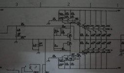
It's the amplifier of VL-200. I see this design stressout on final stages. This amp is robust. The front stage is 3 stages, but after that feed another bias stage and final stage (5 stages all?). The bias/VBE multiplier is unique, reminds me of Lars Clausen's ZETA.
Here's the front stage :
Have you been to Indonesia?😀
It's the amplifier of VL-200. I see this design stressout on final stages. This amp is robust. The front stage is 3 stages, but after that feed another bias stage and final stage (5 stages all?). The bias/VBE multiplier is unique, reminds me of Lars Clausen's ZETA.
Here's the front stage :
Attachments
Unusual indeed, so is the double current source.
My brother in law is from Seram, i have been married to someone part Indonesian, and I am Dutch.
My brother in law is from Seram, i have been married to someone part Indonesian, and I am Dutch.
Got an hour at my prototype today.
Keeping the input stage as 2x BC556B and 2x BC547C only.
The 2x BC557C made the reproduction sound slightly harder.
More soon ........... Graham.
Keeping the input stage as 2x BC556B and 2x BC547C only.
The 2x BC557C made the reproduction sound slightly harder.
More soon ........... Graham.
To keep this on the radar..
Attached is LTSpice file for those who want to simulate it.
In spice it is unstable, unless you turn off semiconductor capacitance. How much of this does it leave it to be trusted?
If you do, it shows incredible linearity. 0.0008% THD at 20W into 8ohms, 2nd harmonic.
I'm not sure of the models I have, but it seems that mirror loaded differential is what is causing ltspice to go bananas.
Attachments
Hi wimms,
Thank you for taking the trouble to report your findings, good to read you can confirm linearity with such a basic circuit.
Progress has not been smooth here.
Increases in rail voltage has increased hf instability.
I fit 'C's to mirror to counter oscillation, but sound is actually too punchy at present.
I shall be trying another bias shunt arrangement tomorrow.
Cheers ........ Graham.
class aabb ltspice sim
wimms,
Nice work!
Is there an error on your schematic?
There is a extra ground symbol at the C5, R6 node.
(near the input transistors Q1, Q2)
Tom
wimms,
Nice work!
Is there an error on your schematic?
There is a extra ground symbol at the C5, R6 node.
(near the input transistors Q1, Q2)
Tom
Re: class aabb ltspice sim
It was done deliberately as per Graham's comments in post http://www.diyaudio.com/forums/showthread.php?postid=580140#post580140 and hints in schematics. I removed decoupling caps basically. It affects only DC offset and causes slight DC drift.Tom2 said:Is there an error on your schematic?
There is a extra ground symbol at the C5, R6 node.
(near the input transistors Q1, Q2)
Hi All,
I am close to giving up on this circuit, because it is not as good at high rail voltages.
I want the good class-A performance with real power, and I'm still not there in real life.
Taking a re-think.
Cheers ......... Graham.
I am close to giving up on this circuit, because it is not as good at high rail voltages.
I want the good class-A performance with real power, and I'm still not there in real life.
Taking a re-think.
Cheers ......... Graham.
Hi Graham,
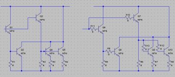
when reading your last post it comes to my mind when you talk about problems with instability, if we take your schematic at least how it looks like in post #21, when I study it, it has a complex formation around output transistors working in class A, AB, B.
Maybe the instability is not about C-dom and such stabilisation things but rather strange instability between these output transistors, they all switch in at diffrent levels of load and it is perhaps so that some transistor initiate others to switch on and off and the instability get's loose.
The PCB layout can also be very critical around this special output stage.
I try to attach a picture, the left is a copy of your schematic, and the right is where small base stoppers is added to each output transistor.
EDIT: Maybe you could try to remove the class B stage and it's driver and see(listen) if you still get the performance you wanted?
What do you think?
Regards Michael
Attachments
Hi Michael.
I can stop the intstability, but living with the sound shows that what I took for impressive attack is actually something unusual.
It is as if the output stage over-compensates for dynamic loading, and what I call the 'punchiness'.
It is unusual, and the exact opposite to the weakness of current drive notable on both mid range and bass at frequencies where I know that driver impedances are low.
The JLH class-A is for current drive, and both upper plus lower driver currents when added can exceed the current flowing through the upper biasing resistors, especially when there is a single input transistor.
I believe that my AABB output stage will need a fixed total drive current to work properly at higher voltages.
When tacked on to my 25W class-A it really was fine. That had 390 ohm collector/emitter drive resistors; to go higher power would have meant a more powerful driver transistor, and again this is a direction I do not want to take.
The old thinking cap has not yet been hung up though. Currently I like the look of Susan's 'non feedback' design , and Mike's 'capacitor-less' circuit.
Have to do other things at the moment, but back soon.
Cheers ........... Graham.
Hi,
I've been playing around with this JLH topology wrt Grahams AABB outputs, and I got interesting result.
Simulation of Graham circuit was unstable in my sim, I guess that this is because of too high gain in the diff stage with accompaning delays and phase shifts. I decided to make it as simple as possible, and went to JLH single input BJT.
Had to remove output offset. Typically this is done by pot biasing input BJT for zero output offset.
I tried different "pot" settings to remove the offset from output. What I observed is that as I approached zero offset, the amp tends to become increasingly unstable. My guess is: As the input BJT needs some bias current to stay active, it must draw some current from the output, there is no other place. JLH output stage is purely current balance, meaning that when offset is exactly zero, there is no current left to bias that input BJT, and it shuts closed. This causes splitter to close and positive outputs to increase current, which in turn opens input BJT again, etc. When there is lag through the amp as is increasingly probable with very low biasing current, oscillations around zero error seem logical. So it seems that this type of zero offset setting has some inherent flaw. It didn't exactly oscillate, but instead had increased output noise. Probably amps output impedance rises as the error voltage approaches zero.
I decided to get away with the cap to ground in the feedback loop and the DC zeroing pot and use DC servo as virtual pot instead. Makes it so much simpler in sims anyway. Just for simplicity of setting input BJT biasing current I added 1ma CCS to negative rail from input BJT collector instead of resistor. Given that this current has to flow from NFB grounded resistor, it causes some DC offset on it, few mV for Kohm NFB resistors, and that also draws from output. But it does not depend on output error voltage this way, and thus has no effect on output impedance when error voltage approaches zero.
Things got interesting for me when I noticed that resistor from the splitter emitter to rail increases THD. I realise that this output stage base pulldown resistor must increase the slew rate of the amp, and somewhat compensate for splitter base current, but in reality it modulates the output stage idle bias current so that during positive going wave it draws more from bootstrap or idle CCS than during negative going wave. This causes asymmetry with large signal and corresponding THD increase. I tried replacing it with ideal CCS, but it does not show any notable improvement. Instead, I found that best result is achieved when that pulldown resistor is simply omitted. That doesn't feel right, although classical darlington works like this. I wonder what bad will happen without one?
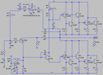
Attached is a circuit I got, using JLH topology with Graham's class-AABB output stage. It has 80W idle with 1Amp idle current, and in simulations with models I have and parasitics included gives 0.001% THD into 8ohm resistive load at 27W, and 0.005% THD into same load at 196W (swing to 2V within rails). IMD below -100db. very effective back-EMF handling. I tried with speakerload model. It seems to very effectively damp backEMF by feeding error current back directly through splitter and also input BJT.
Dunno if there is anything new in this circuit. NFB grounding R1 is used also to bias input BJT Q1. For that CCS of 1ma in Q1 collector is used. This CCS biases the Q1 and also removes the bias current before splitter. Thus splitter gets basically only amplified input AC current with NFB error current subtracted, plus bias set by DC-servo based on output offset. Interesting is the R7 in parallel with CCS. Its value has been found by picking. There is a specific value of it when THD is lowest. I'm not sure why. Emitter resistor of splitter is removed. Anything there and THD goes up.
R1 and NFB values are very low. There can be 15W burned on the NFB R7, but low ohms of R1 is good.
Interestingly, boostrap gives better THD results in sim than ideal CCS of equal current in this circuit. Strange. I wonder if the voltage drop on the boostrap resistor is somewhat compensating nonlinearity of splitter bjt.
Interesting is that removing class-B stage from the mix actually increases THD which was for me unexpected. It seems to reduce output impedance for good, in a weird manner, by starving opposite legs base current through splitter by showing reduced impedance to bootstrap ccs.
I'd like to hear your reasoning on why low impedance NFB network has positive impact on THD, is the splitter without emitter resistor viable solution, and what is the real reason why 1m CCS shunt resistor needs be picked and is the bootstrap really prefered CCS as sim seems to suggest? I have my "theory" on these matters, but I'd rather listen to those who know better. I think it has to do with how currents circulate from output back to splitter and how much of error signal is lost.
When I stepped NFB ground resistor as 10, 100, 1k, keeping FB resistor 20x larger, I observed that propagation delay increases with impedance. Thus low NFB impedance looking into input BJT emitter seems prefered. It also reduces over-compensation, which seems to be simply late compensation. This low impedance NFB benefits both, with grounded capacitor and without. I've not seen it done this way.
I've been playing around with this JLH topology wrt Grahams AABB outputs, and I got interesting result.
Simulation of Graham circuit was unstable in my sim, I guess that this is because of too high gain in the diff stage with accompaning delays and phase shifts. I decided to make it as simple as possible, and went to JLH single input BJT.
Had to remove output offset. Typically this is done by pot biasing input BJT for zero output offset.
An externally hosted image should be here but it was not working when we last tested it.
I tried different "pot" settings to remove the offset from output. What I observed is that as I approached zero offset, the amp tends to become increasingly unstable. My guess is: As the input BJT needs some bias current to stay active, it must draw some current from the output, there is no other place. JLH output stage is purely current balance, meaning that when offset is exactly zero, there is no current left to bias that input BJT, and it shuts closed. This causes splitter to close and positive outputs to increase current, which in turn opens input BJT again, etc. When there is lag through the amp as is increasingly probable with very low biasing current, oscillations around zero error seem logical. So it seems that this type of zero offset setting has some inherent flaw. It didn't exactly oscillate, but instead had increased output noise. Probably amps output impedance rises as the error voltage approaches zero.
I decided to get away with the cap to ground in the feedback loop and the DC zeroing pot and use DC servo as virtual pot instead. Makes it so much simpler in sims anyway. Just for simplicity of setting input BJT biasing current I added 1ma CCS to negative rail from input BJT collector instead of resistor. Given that this current has to flow from NFB grounded resistor, it causes some DC offset on it, few mV for Kohm NFB resistors, and that also draws from output. But it does not depend on output error voltage this way, and thus has no effect on output impedance when error voltage approaches zero.
Things got interesting for me when I noticed that resistor from the splitter emitter to rail increases THD. I realise that this output stage base pulldown resistor must increase the slew rate of the amp, and somewhat compensate for splitter base current, but in reality it modulates the output stage idle bias current so that during positive going wave it draws more from bootstrap or idle CCS than during negative going wave. This causes asymmetry with large signal and corresponding THD increase. I tried replacing it with ideal CCS, but it does not show any notable improvement. Instead, I found that best result is achieved when that pulldown resistor is simply omitted. That doesn't feel right, although classical darlington works like this. I wonder what bad will happen without one?
Attached is a circuit I got, using JLH topology with Graham's class-AABB output stage. It has 80W idle with 1Amp idle current, and in simulations with models I have and parasitics included gives 0.001% THD into 8ohm resistive load at 27W, and 0.005% THD into same load at 196W (swing to 2V within rails). IMD below -100db. very effective back-EMF handling. I tried with speakerload model. It seems to very effectively damp backEMF by feeding error current back directly through splitter and also input BJT.
Dunno if there is anything new in this circuit. NFB grounding R1 is used also to bias input BJT Q1. For that CCS of 1ma in Q1 collector is used. This CCS biases the Q1 and also removes the bias current before splitter. Thus splitter gets basically only amplified input AC current with NFB error current subtracted, plus bias set by DC-servo based on output offset. Interesting is the R7 in parallel with CCS. Its value has been found by picking. There is a specific value of it when THD is lowest. I'm not sure why. Emitter resistor of splitter is removed. Anything there and THD goes up.
R1 and NFB values are very low. There can be 15W burned on the NFB R7, but low ohms of R1 is good.
Interestingly, boostrap gives better THD results in sim than ideal CCS of equal current in this circuit. Strange. I wonder if the voltage drop on the boostrap resistor is somewhat compensating nonlinearity of splitter bjt.
Interesting is that removing class-B stage from the mix actually increases THD which was for me unexpected. It seems to reduce output impedance for good, in a weird manner, by starving opposite legs base current through splitter by showing reduced impedance to bootstrap ccs.
I'd like to hear your reasoning on why low impedance NFB network has positive impact on THD, is the splitter without emitter resistor viable solution, and what is the real reason why 1m CCS shunt resistor needs be picked and is the bootstrap really prefered CCS as sim seems to suggest? I have my "theory" on these matters, but I'd rather listen to those who know better. I think it has to do with how currents circulate from output back to splitter and how much of error signal is lost.
When I stepped NFB ground resistor as 10, 100, 1k, keeping FB resistor 20x larger, I observed that propagation delay increases with impedance. Thus low NFB impedance looking into input BJT emitter seems prefered. It also reduces over-compensation, which seems to be simply late compensation. This low impedance NFB benefits both, with grounded capacitor and without. I've not seen it done this way.
Attachments

Hi Wimms,
I'm reet chuffed that my AABB output arrangement is not being ignored.
I believe my mistake to date has been applying current drive instead of voltage drive in my attempt to use the low distortion JLH output arrangement.
In an output stage the stage gain falls as the voltage across the conducting half falls with increasing amplitude; this is not the same as simplistic device gain as viewed from specification sheets. The additional class-B device 'compensates' for the fall in gain with increased current demands at high amplitude. The 2x class-ABs do most of the work, leaving the class-As running linearly without ever going off (if properly biased) whereupon they can maintain linearity through the two different time/voltage AB and B conductions.
Suggestion;- add another transistor to the CCS so that you double up on Q2, and use this to sink some standing current through the BD139.
Also see (attached) the four transistor circuit I recently posted in the 10W JLH class-A column for an input biasing arrangement that has proved convenient in real life, even with this output stage too.
Adding the driver emitter resistor is increasing distortion because your bootstrapped collector resistors have equal value. The upper one is better being much lower in the JLH output stage.
Lower resistance at the input transistor emitter reduces thd by increasing the ratio between emitter resistance and R7/Q7 resistance/impedance; ie. increasing stage gain.
The FFT is not bad considering how badly balanced your investigative circuit is.
And the big question; are you adventurous enough to try it in real life ?
Cheers ........... Graham.
- Status
- Not open for further replies.
- Home
- Amplifiers
- Solid State
- Class-AABB output stage.