I have a preamp I would like to build but I have yet to decide whether to use a choke loaded PSU or a VR tube regulated PSU. Does anyone have any first hand experience with both? Which did you prefer?
Actually, I use both. At the end of the day, the choke was unnecessary, and just added additional cost, weight, and magnetic field issues.
Were I to do it again, I would run the IXYS 10M45S as a current source into the VR tube, losing the choke. Ripple is essentially zero.
I should mention, however, that my linestage is a differential design, not single ended. YMMV when dealing with a single ended topology.
Were I to do it again, I would run the IXYS 10M45S as a current source into the VR tube, losing the choke. Ripple is essentially zero.
I should mention, however, that my linestage is a differential design, not single ended. YMMV when dealing with a single ended topology.
zigzagflux said:Actually, I use both. At the end of the day, the choke was unnecessary, and just added additional cost, weight, and magnetic field issues.
Were I to do it again, I would run the IXYS 10M45S as a current source into the VR tube, losing the choke. Ripple is essentially zero.
I should mention, however, that my linestage is a differential design, not single ended. YMMV when dealing with a single ended topology.
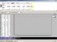
I appreciate your reply. I have been trying to utilize PSU Designer II to help design a shunt regulated supply using a OD3 without much luck. How did you make your calculations?
I tried modeling the psu using the VR tube and the 15K load in parrallel as a 4.615K load. I wish the program would allow you to use VR tubes in the model.
G said:Screw it. I will just use the choke loaded supply.
Patience, friend. The rewards are worth it, IMO. Realtor coming over tonite, I'll spend a little time modeling one for you later.
G said:I have a preamp I would like to build but I have yet to decide whether to use a choke loaded PSU or a VR tube regulated PSU. Does anyone have any first hand experience with both? Which did you prefer?
why not both ?
that's at least what I prefer
There'd be no harm to both.
I personally have no VR, just CLCR(i1)CR(i2)C and *hopefully* it should be fine
I personally have no VR, just CLCR(i1)CR(i2)C and *hopefully* it should be fine
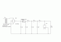
This is my power supply for a Raven style DAC/preamp. As I mentioned, it is a choke loaded supply, which I might not pursue if I were to do it again. As far as using PSUD for the design, I will explain what I've done:
C1-L1-C2 is the typical starting point for the filter. R2 was placed in order to reduce the dissipation of the current source, which is directly after R2. This was due to the fact that I wanted to experiment with different VR tubes and operating points, so R2 gives me a little wiggle room and tweakability.
C3 is completely optional, and even unnecessary. Had the space, decided to put it in.
First current source is the left channel current source. It is placed where it is to simulate the loading on the overall power supply.
The 300 ohm R3 resistor "simulates" the right channel current source. It is selected to produce the VR nominal voltage across C4/I2. If the voltage is incorrect, I tweak R3 until it is correct. Then, I am able to calculate a few things: one, the dissipation in the current source, which is the same as the dissipation in R3. Two, I am able to check the peak output voltage the current source can provide to the load PRIOR to the VR striking. In the example, this is 127V minus the minimum drop of the CCS, around 4V. So my voltage during startup will rise as high as 123V. If my VR doesn't strike at this voltage or lower, it will never strike.
If I need to adjust this available striking voltage, I can do it with R2 changes. A smaller R2 will increase the available striking voltage, while also increasing the dissipation in my CCS.
Actual installation does not include R3 - instead it is replaced by your CCS. As you can tell, this design uses the 0C3/VR105 regulator.
With this approach, PSUD gave me results within about 2V. Ripple values within maybe 10mV.
Attachments
zigzagflux said:This is my power supply for a Raven style DAC/preamp. As I mentioned, it is a choke loaded supply, which I might not pursue if I were to do it again. As far as using PSUD for the design, I will explain what I've done:
C1-L1-C2 is the typical starting point for the filter. R2 was placed in order to reduce the dissipation of the current source, which is directly after R2. This was due to the fact that I wanted to experiment with different VR tubes and operating points, so R2 gives me a little wiggle room and tweakability.
C3 is completely optional, and even unnecessary. Had the space, decided to put it in.
First current source is the left channel current source. It is placed where it is to simulate the loading on the overall power supply.
The 300 ohm R3 resistor "simulates" the right channel current source. It is selected to produce the VR nominal voltage across C4/I2. If the voltage is incorrect, I tweak R3 until it is correct. Then, I am able to calculate a few things: one, the dissipation in the current source, which is the same as the dissipation in R3. Two, I am able to check the peak output voltage the current source can provide to the load PRIOR to the VR striking. In the example, this is 127V minus the minimum drop of the CCS, around 4V. So my voltage during startup will rise as high as 123V. If my VR doesn't strike at this voltage or lower, it will never strike.
If I need to adjust this available striking voltage, I can do it with R2 changes. A smaller R2 will increase the available striking voltage, while also increasing the dissipation in my CCS.
Actual installation does not include R3 - instead it is replaced by your CCS. As you can tell, this design uses the 0C3/VR105 regulator.
With this approach, PSUD gave me results within about 2V. Ripple values within maybe 10mV.
Interesting. Below is my starting point for the PSU. I need 150v @ 10mA. The I mean for the OD3 is 22.5mA. If I parrallel the load and the current draw of the OD3 I get a 4.615K load. I guess all I need to adjust is R1, R2 and R3 to get about 180v @ 32.5mA at the anode of the OD3 huh?
Attachments
Hmmmmm. Let's back up a little.
If we simply model your first CLC stage, and I have taken the liberty of using a 47uF cap for C2 (which I recommend), and insert a 30mA current source on the output (VR current + load current), your voltage at C2 is only 158V. This will not be nearly enough to get your VR to fire, nor will it allow for any line/load regulation.
I had to increase C1 to 10uF, which brought the voltage at C2 up to about 200V. Now we are in the ballpark for using a 150V regulator tube.
Are you with me so far? If not, we can't really go any further.
zigzagflux said:Hmmmmm. Let's back up a little.
If we simply model your first CLC stage, and I have taken the liberty of using a 47uF cap for C2 (which I recommend), and insert a 30mA current source on the output (VR current + load current), your voltage at C2 is only 158V. This will not be nearly enough to get your VR to fire, nor will it allow for any line/load regulation.
I had to increase C1 to 10uF, which brought the voltage at C2 up to about 200V. Now we are in the ballpark for using a 150V regulator tube.
Are you with me so far? If not, we can't really go any further.
Yes. I am with you. I see that I did not put in the values for the capacitors. They are all 100uF capacitors.
Hi Guys,
You're missing out the point of Chokes in PS.
Putting aside cost, aside from smoothing the ripple,
it does wonders to music reproduction.
Talk to guys who have played around with chokes.
I'm sure they will say the same.
You're missing out the point of Chokes in PS.
Putting aside cost, aside from smoothing the ripple,
it does wonders to music reproduction.
Talk to guys who have played around with chokes.
I'm sure they will say the same.
Okay G:
This transformer is a little marginal for the design, but it could be because I do not have the actual parameters modelled correctly in PSUD. I am using 165V at 150 ohm for it. What do you have?
Reason I bring this up is because if I put in your 100u and 100u caps, take a look at V(T1). It is flap topped, indicating the regulation of the transformer has severely limited your output. You obviously want to avoid this condition. You will be faced with this problem regardless if you go with a CCS or not. The CLC is causing it, along with your rated load.
To attempt to remedy it, I have reduced C1 to 3.3 uF, keeping C2 at 100uF. Also reduced your total load to 25mA (10mA load + 15 mA VR). Now, things look much better, though still a little warping of the voltage. Tolerable, IMO, but a cheaper transformer might be making some noise.
With C1 reduced to 3.3uF, I still get 200V at C2, indicating the huge C1 is not really necessary (and in fact makes things worse). Let the choke do its job. Keep C1 small, and maybe higher quality film. Not expensive in this size.
Attached is a tentative design. The 2K resistor will be replaced by your CCS. Note ahead of it, at C2, is 200V, and downstream, at C3, is 150V (0D3 regulated voltage).
I should mention that earlier I stated ripple within 10mV. This is not the ripple present on my regulated B+. There, it is uV. I was simply showing that upstream in the filter section, the ripple I was gettting in PSUD was predicting within 10mV the actual measured ripple. This program is unbelievably accurate, and can be trusted for these simple power supplies. We can get into stability later 🙂
Attachments
zigzagflux said:Okay G:
This transformer is a little marginal for the design, but it could be because I do not have the actual parameters modelled correctly in PSUD. I am using 165V at 150 ohm for it. What do you have?
Reason I bring this up is because if I put in your 100u and 100u caps, take a look at V(T1). It is flap topped, indicating the regulation of the transformer has severely limited your output. You obviously want to avoid this condition. You will be faced with this problem regardless if you go with a CCS or not. The CLC is causing it, along with your rated load.
To attempt to remedy it, I have reduced C1 to 3.3 uF, keeping C2 at 100uF. Also reduced your total load to 25mA (10mA load + 15 mA VR). Now, things look much better, though still a little warping of the voltage. Tolerable, IMO, but a cheaper transformer might be making some noise.
With C1 reduced to 3.3uF, I still get 200V at C2, indicating the huge C1 is not really necessary (and in fact makes things worse). Let the choke do its job. Keep C1 small, and maybe higher quality film. Not expensive in this size.
Attached is a tentative design. The 2K resistor will be replaced by your CCS. Note ahead of it, at C2, is 200V, and downstream, at C3, is 150V (0D3 regulated voltage).
I should mention that earlier I stated ripple within 10mV. This is not the ripple present on my regulated B+. There, it is uV. I was simply showing that upstream in the filter section, the ripple I was gettting in PSUD was predicting within 10mV the actual measured ripple. This program is unbelievably accurate, and can be trusted for these simple power supplies. We can get into stability later 🙂
I am not following. The transformer is rated at 150mA with both winding in parallel. That is about five times what this circuit will draw, with the OD3, at idle. Below is the PSU I was going to use before I started thinking about regulating it.
Attachments
Above you mentioned Hammond 379BX. I don't see that xfmr anywhere on their website. Do you have any data on it?
Regardless, you should see that the peak currents drawn by the first capacitor are well in excess of 150mA when you have the 100uF size installed. That is why the output is sagging. Very typical with capacitor input filters. That is why I recommended lowering the value.
With the design you provided, take a look at V(T1) and I(T1). Very informative.
zigzagflux said:Above you mentioned Hammond 379BX. I don't see that xfmr anywhere on their website. Do you have any data on it?
Regardless, you should see that the peak currents drawn by the first capacitor are well in excess of 150mA when you have the 100uF size installed. That is why the output is sagging. Very typical with capacitor input filters. That is why I recommended lowering the value.
With the design you provided, take a look at V(T1) and I(T1). Very informative.
I apologize. The transformer is a 369BX. All I ever look at is the voltage or current supplied to the load. If lowering C1 will help with regulation then by all means proceed.
Also. I have not purchased the power transformer nor the choke yet so changing the transformer in the model is not a problem. However I am trying to stay with the "X6" sized transformer. You obviously know much more about PSU design than I so by all means feel free to use any 300 series transformer needed. Since I will be using a Ixys bridge you can assume that both windings will be connected in parallel thereby doubling the current rating used for a full wave rectifier. By the way, how did you lower the size of the image of PSUD enough to get the board to accept it?
Very good. That will work. It is actually a center tapped winding, so in PSUD you need to change the rectifier topology to solid state Full Wave, not Bridge. You will get the same result essentially, but only need two diodes instead of four.
I modeled an approximate impedance for the transformer. You would have to measure yours to get more accurate. Close enough for the discussion.
Note that C2 is just under 200V. This is all you have available to fire the VR tube. This is sufficient. Data sheet recommends 185 minimum.
The value for C1, as discussed earlier, affects the voltage at C2. Larger capacitance results in higher C2 voltage, but also higher peak currents through the transformer (which is bad). Values from 3.3 to 4.7 seem to work good, but going as low as 2.2 seems to lower C2 voltage too much for reliable striking. Go for at least 3uF. Pick your favorite capacitor; I like a Solen or CDE 940C; even a 'lytic is fine (*ducks head*). 400V
Again, R1 is the simulated current source. V(R1) is 46V, so your current source will dissipate 46 * 0.025 = 1.15W. No problem; that's a small heatsink, and is cheap for the tight regulation you get. Even under short circuit (disaster) conditions, you only dissipate 5W. A durable design.
Okay, we know the static conditions are fine. VR will take 15 mA, load 10 mA. The tricky part is verifying a successful strike. To do this, you have to look at your load characteristic. In order for the VR to strike, it needs ABOUT 180V, and will vary quite significantly from tube to tube. Therefore, your load voltage will rise from zero to around 180V, without any current being consumed by your VR. Question is, how much current does the LOAD consume at this elevated voltage? If it is equal or greater than 25 mA (all that is available from the CCS), the VR will not strike. If it is only, say 20mA, then the CCS will attempt to drive the full 25 mA, continuing to raise the voltage (up to max 200V) until the VR does strike.
Hope this makes sense. I have designed shunt regulated circuits with resistors that failed to strike for this very reason, so I consider it important to check the startup behavior. Using a CCS makes the calculations easier, of course.
That's about it; I wouldn't add any more components than this. Plenty of threads about CCS design if you need help there.
Two questions, though:
1. Is this a monoblock design, or stereo, where you actually need 2 * 25 mA ?
2. What type of load are we dealing with? Is the consumption essentially constant regardless of music content?
Attachments
zigzagflux said:Very good. That will work. It is actually a center tapped winding, so in PSUD you need to change the rectifier topology to solid state Full Wave, not Bridge. You will get the same result essentially, but only need two diodes instead of four.
I modeled an approximate impedance for the transformer. You would have to measure yours to get more accurate. Close enough for the discussion.
Note that C2 is just under 200V. This is all you have available to fire the VR tube. This is sufficient. Data sheet recommends 185 minimum.
The value for C1, as discussed earlier, affects the voltage at C2. Larger capacitance results in higher C2 voltage, but also higher peak currents through the transformer (which is bad). Values from 3.3 to 4.7 seem to work good, but going as low as 2.2 seems to lower C2 voltage too much for reliable striking. Go for at least 3uF. Pick your favorite capacitor; I like a Solen or CDE 940C; even a 'lytic is fine (*ducks head*). 400V
Again, R1 is the simulated current source. V(R1) is 46V, so your current source will dissipate 46 * 0.025 = 1.15W. No problem; that's a small heatsink, and is cheap for the tight regulation you get. Even under short circuit (disaster) conditions, you only dissipate 5W. A durable design.
Okay, we know the static conditions are fine. VR will take 15 mA, load 10 mA. The tricky part is verifying a successful strike. To do this, you have to look at your load characteristic. In order for the VR to strike, it needs ABOUT 180V, and will vary quite significantly from tube to tube. Therefore, your load voltage will rise from zero to around 180V, without any current being consumed by your VR. Question is, how much current does the LOAD consume at this elevated voltage? If it is equal or greater than 25 mA (all that is available from the CCS), the VR will not strike. If it is only, say 20mA, then the CCS will attempt to drive the full 25 mA, continuing to raise the voltage (up to max 200V) until the VR does strike.
Hope this makes sense. I have designed shunt regulated circuits with resistors that failed to strike for this very reason, so I consider it important to check the startup behavior. Using a CCS makes the calculations easier, of course.
That's about it; I wouldn't add any more components than this. Plenty of threads about CCS design if you need help there.
Two questions, though:
1. Is this a monoblock design, or stereo, where you actually need 2 * 25 mA ?
2. What type of load are we dealing with? Is the consumption essentially constant regardless of music content?
The circuit is essentially a Foreplay preamp using 6SN7s. The current draw will be 5mA per side and since it is a class A there is not going to be much variation in the load.
- Status
- Not open for further replies.
- Home
- Amplifiers
- Tubes / Valves
- Choke loaded PSU versus VR tube regulated PSU?