Yes, the low supply voltage makes it no good to use verticals.
The low voltage is for suit the opamp.
I have this one with +/-25 Volt.
It might be good for verticals.
The low voltage is for suit the opamp.
I have this one with +/-25 Volt.
It might be good for verticals.
Sioux
Here is a higher power version of Choctaw.
Output 26 Watt with +/-25VDC supply.

Here is a higher power version of Choctaw.
Output 26 Watt with +/-25VDC supply.
- lineup
- Replies: 102
- Forum: Solid State

Last edited:
I did it using a Zoltan's board.
I had some issues with cross channel hum so HBR (hum breaking resistor) was needed in my case.
I have cut GND trace and add 20R resistance between input/fb ground and PS capacitors.
Answer my own question. I measured a pair of 2SK1057, 2SJ161. They are biased at 100mA each at 0.5Vgs. Thus, 1.2V battery would be too much.How much is gate bias voltage? I want to see if it works with two 1.2v NiMH batteries to bias the gate.
Below I borrow the IV chart from ECX10N20. They are very closed to the original 2SK1058 family. With 0.7v, it biases between 150mA and 200mA, very practical.
Last edited:
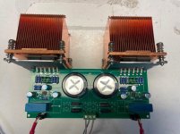
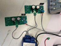
A month ago I have built the amplifier according to the schematic titled "Choctaw_21 final" on post 322, with the gerber supplied by Zoltan. I have done only a few basic tests on the bench. There is a slight hum on the left channel when both inputs are shorted to ground. Right channel is silent. At first I thought that the hum would be gone when the board is properly assembled inside the chassis and I've put everything aside while I'm waiting for it. Today I've done a few more tests, and the hum is coming from the power supply: it stops when I cut the power on the primary side of the power transformer. It does not go away or change amplitude when I place the transformer at a distance. I cannot evaluate the sonic quality of my build yet because I also experience the issue described by Benpe: when I connect only one channel, the amplifier works; as soon as I connect the second channel, loud hum starts on both channels. I will probably disassemble the left channel components from the board and reuse them to populate the right channel of one of the spare boards I have, so I will also solve the background hum noise issue. I just need to order two more filter capacitors, they are 25V 15000uF on my build, while the small electrolytics are all 100uF polimeric.
I will try to increase a bit the op amp gain because I will use this amplifier with a portable USB DAC, with lower than usual output: I plan to increase the feedback resistor R6, from 10K to 18K or 22K.
Attachments
Sorry to hear about the problems with this PCBI
'll try to get back to this project soon
I should have the PCB somewhere
'll try to get back to this project soon
I should have the PCB somewhere
If you have used "old" pcb design.There is a slight hum on the left channel when both inputs are shorted to ground. Right channel is silent.
Did you notice missing GND connection at the one of the inputs?
Disconnect the input plug and check connectivity of each of input socket grounds.
Your PCB is still a good way to quickly test this interesting circuit. I am using your latest version, both input socket grounds are connected. If you plan to revise it, I have a few minor suggestions:Sorry to hear about the problems with this PCBI
'll try to get back to this project soon
I should have the PCB somewhere
The writings on the upper copper layer would be more visible if moved to the silkscreen layer.
The pin 1 mark on the silkscreen for the operational amplifier package is tiny and on the opposite orientation of the IC4 marking, I had to double check the traces to be sure.
The power supply traces on the power mosfet side are touching the PCB border. I will put a kapton tape on the heatsink to provide some extra insulation, but a 1mm of space between the traces and the border would have been better.
My preferred low voltage input capacitors are the box type Wima and Epcos with 5 mm leg spacing. On this build I had to use a high voltage one because the smallest spacing for this part on the PCB is 10 mm.
One of the electrolytic capacitors on the left channel is rotated in the opposite direction to the corresponding one on the right channel. When I heard the hum, I was briefly thinking that I had mistakenly inserted the capacitor the wrong way around. It would be best to have all capacitors on the same orientation.
I was unable to find a 10pF NP0 THT capacitor with 2.5mm leg spacing, most common ones have 5mm leg spacing because they are high voltage types. I ended up using a SMD capacitor placed on the holes meant for the traditional capacitor. Due to the very small value a SMD capacitor is easier and cheaper to source, but I guess that the traces are already a significant fraction of this value.
The small electrolytics on the operational amplifier supply rails aren't really needed, they are very close to the way overspecced main capacitors and the opamp does have a pretty high power supply rejection ratio. But since they are there, I would have put a small filter inductor or a low value resistor between the main capacitor and each of the opamp filter capacitors.
The 1W TE connectivity ROX1 film resistors are squeezed on this board, but the decision to use them is a self inflicted discomfort because I use this type of resistor on most of my builds with good results and I wanted to use it on this one also.
Thank you for your commentsYour PCB is still a good way to quickly test this interesting circuit
I will definitely take your suggestions into account in future projects
I don't know if I will revise this project.
issue described by Benpe: when I connect only one channel, the amplifier works; as soon as I connect the second channel, loud hum starts on both channels.
I had experienced similar behavior several times in the past (with different amps).
Each channel was working fine on its own, but when both channels were powered on, the bahavior of amps becomes
erratic (hum, noise, blowing fuses, etc...).
Basically what was happening - amps were osciallating when both channels were powered on.
Since all the cabling, grounding, etc... was always consistent with the rest of my amps, it all came down to insufficient stability of the amp design.
Not sure if this is the case here, but symptoms are similar.
Perhaps there is a way to isolate both channels, to make it work, but I decided against it, and went back to the 'design board' to make them more stable.
This was usually happening on 'cutting edge' fast amps, with slew rate over 120 V/us - which are obviously more prone to oscillations.
I used Irfz40 and irf9z40 back 30 years ago in the car. A LF353 with those fets provides 40w into 4 ohms from 13.8v
No sense using high RDS ON mosfets at such low voltages.
Lower distortion opa2134 should work well.
No sense using high RDS ON mosfets at such low voltages.
Lower distortion opa2134 should work well.
If it is as minek123 writes, it is my fault - I did not check the prototype thoroughly enough before publishing the PCB design.
In the next few days I will try to go back to the prototype and check it for oscillations
In the next few days I will try to go back to the prototype and check it for oscillations
What was the phase margin and gain margin of this amp? How about slew rate ? Was it fast?
My amps with the behavior I described in post #370 - they did simulate OK.
I don't build amps with PM below 50 - that's 'good enough' for most of amps,
but it seems that for faster amps it's not enough.
Also for such fast amps, proper PCB design is also very important, so maybe I failed in that area.
Never the less, for fast amps, I aim at PM > 60 now, which is not easy.
Last edited:
What was the phase margin and gain margin of this amp? How about slew rate ? Was it fast?
I did a quick sim in LTSpice based on bohrok's sim, and there it is:
Thd: 0.0011% (really irrelevant...)
Estimated Slew Rate: 14V/us - more than enough for 10W amp.
Squares look perfect - but if someone plans to add RC filter at input, this would have to be re-simed with a specific filter.
PM: 101, GM: 27 - somehow these numbers look 'too high', but maybe they are correct? No idea. Bottom line - I've never seen
numbers this high on any amp. If they are correct, that's great. Can someone verify this in LtSpice?
Basically they look like 'perfect' OLG plots for op-amp alone; we often see...
SR is slow. Not a reason of oscillations.
PM number of 101 is in my opinion wrong.
Never seen an amp with PM over 80. Anybody confirmed these numbers?
PM number of 101 is in my opinion wrong.
Never seen an amp with PM over 80. Anybody confirmed these numbers?
Looking at the OLG plot from my old post that Zoltan found - it definitely looks suspicious.
Not like most of OLG plots for this kind of amps.
I think these numbers (PM/GM) are not real.....
Not like most of OLG plots for this kind of amps.
I think these numbers (PM/GM) are not real.....
I revisited the sim from post #211, and I don't see if there is anything wrong with it or not.
The only thing is that it looks different (e.g. flatter) than typical plots of this kind, and the numbers (PM/GM) are unusually high.
The unusual look might be a result of the fact that there is no VAS, just an op-amp plus current amplifier (LatFets),
so all voltage gain is realized in the opamp.
The only thing is that it looks different (e.g. flatter) than typical plots of this kind, and the numbers (PM/GM) are unusually high.
The unusual look might be a result of the fact that there is no VAS, just an op-amp plus current amplifier (LatFets),
so all voltage gain is realized in the opamp.
I remember when I built the prototype it had no symptoms of oscillation
I also had no problems with hum or hum....
I want to check this amplifier again
I found an old PCB but I don't have LatFet at the moment.
I use the test set in the prototype of the Sioux amplifier which I am currently testing
I will come back to it after I finish playing with Sioux
I hope that despite the strange simulation results (PM, OLG) it is safe
A quick update on my tests: there is no background hum when I use two PCBs, one for the left and one for the right channel. I also did not found oscillations at the outputs. Audio quality seems fine at low volume but I haven't connected good speakers yet. I will make more measurement after replacing the heatsinks and mounting the boards and the transformer in a temporary enclosoure. Heat dissipation at idle is lower than expected; I will try to use smaller heatsinks.
Attachments
- Home
- Amplifiers
- Solid State
- Choctaw - 10 Watt Amplifier, 1 Opamp + 2 MOSFET