Hi,
Sorry but I don't see how you can even discuss something as obvious as this.
To prove the effect: take a simple triode cathode biased with a resistor.
Bypass that resistor, you create an AC short to ground: no feedback.
Remove the cap and the gain of that stage will drop, the stage will be linearised hence show less distortion.
As a side effect Rp goes up so Zout will go up too but that's besides the point.
I think the discussion was about whether this is voltage feedback or current feedback though...IIRC.
Form a marketing POV, the way I perceive it, when the leaflet says no feedback used, they often refer to the fact that no GLOBAL FB loop is employed.
Global meaning from the output of the amp (usually the + LS terminal) to the input of the amp, encompassing every stage within that loop.
This usaually also means that all kinds of other methods are employed to reduce distortion and lower output impedance to "acceptable" (whatever those are) levels.
Those methods can vary from a local loop around a single active device to loops around compound gainblocks, around the output stage only, parallelled devices, any combination of the thinkable, etc, etc....ad nauseam.
Of course, all this discussion wouldn't be necessary if the marketing guys would have been more informative and had said : no global feedback loop employed iso of saying no feedback.
Whether it would have sold the idea in the same way, I very much doubt....
Cheers,😉
I have actually got the impression that has been the cause of previous heated debates, but maybe i missed the point
in those discussions.
Sorry but I don't see how you can even discuss something as obvious as this.
To prove the effect: take a simple triode cathode biased with a resistor.
Bypass that resistor, you create an AC short to ground: no feedback.
Remove the cap and the gain of that stage will drop, the stage will be linearised hence show less distortion.
As a side effect Rp goes up so Zout will go up too but that's besides the point.
I think the discussion was about whether this is voltage feedback or current feedback though...IIRC.
Let's say that zero feedback is when we have no feedback loop spanning more than one amplifier stage. Do you agree to that, or do only certain types of local feedback within a
stage qualify?
Form a marketing POV, the way I perceive it, when the leaflet says no feedback used, they often refer to the fact that no GLOBAL FB loop is employed.
Global meaning from the output of the amp (usually the + LS terminal) to the input of the amp, encompassing every stage within that loop.
This usaually also means that all kinds of other methods are employed to reduce distortion and lower output impedance to "acceptable" (whatever those are) levels.
Those methods can vary from a local loop around a single active device to loops around compound gainblocks, around the output stage only, parallelled devices, any combination of the thinkable, etc, etc....ad nauseam.
Of course, all this discussion wouldn't be necessary if the marketing guys would have been more informative and had said : no global feedback loop employed iso of saying no feedback.
Whether it would have sold the idea in the same way, I very much doubt....
Cheers,😉
I dont understand this
Charles Hansen wrote this :
From what I know, Trans Nova is some kind of inverted output, where the output transistors are emitor followers, but it's emitors are connected to ground, so the output is taken from the CT of the transformer.
How come you said this is the same as Hawksford error correction? I dont see any similiarities between these two.
Charles Hansen, come in please!
Charles Hansen wrote this :
4) The error correction circuit published by Hawksford is also a feedback circuit. The loop is typically just around the output stage, so it is shorter than a "global" feedback loop, but longer than the loop of a CFP. The twist is that there is gain in the *reverse* direction of this loop. This technique was first used (to the best of my knowledge) in the early Quad solid state amp that they called the "current dumping" circuit (I forget the model number). It was also used in the "Trans Nova" circuit that Jim Strickland did for Acoustat and later Hafler. However, the Hawksford paper formalized this approach, explained it, and made it easy to adapt to existing output stages
From what I know, Trans Nova is some kind of inverted output, where the output transistors are emitor followers, but it's emitors are connected to ground, so the output is taken from the CT of the transformer.
How come you said this is the same as Hawksford error correction? I dont see any similiarities between these two.
Charles Hansen, come in please!
For Mr. PASS
Mr. Pass,
Is that your patent no. 3,995,228 is the same thing as Hawksford error correction? Or is it aiming at different purpose?
Mr. Pass,
Is that your patent no. 3,995,228 is the same thing as Hawksford error correction? Or is it aiming at different purpose?
Differential
Audio is very interesting. At first I'm amazed by complex designs. As time pass, I raise question about more and more simple things. Like this one.
In Doug Self book, he takes great care on balancing 2 transistor in differential. If the CCS is 4mA, he studies that each transistor will bias at 2mA. He comes up with current mirror.
How important is it to have the exact bias current splitted between these 2 differential transistor?
If I have differential not working very balance, like one is biased 1mA and the other is 3mA, but Thermally Coupled, how bad is it?
Is that splitting bias equally between 2 differential transistor is a must?
Hi,
There's little point in going differential if you don't except for some very special occasions where you'd do that on purpose...
If you work with low tolerance devices you'll probably have to set bias individually to preserve correct differential operation.
Again, this will all depend on what your goals are but generally speaking, this is what you'd do.
Cheers, 😉
Is that splitting bias equally between 2 differential transistor is a must?
There's little point in going differential if you don't except for some very special occasions where you'd do that on purpose...
If you work with low tolerance devices you'll probably have to set bias individually to preserve correct differential operation.
Again, this will all depend on what your goals are but generally speaking, this is what you'd do.
Cheers, 😉
fdegrove said:Form a marketing POV, the way I perceive it, when the leaflet says no feedback used, they often refer to the fact that no GLOBAL FB loop is employed.
Global meaning from the output of the amp (usually the + LS terminal) to the input of the amp, encompassing every stage within that loop.
This usaually also means that all kinds of other methods are employed to reduce distortion and lower output impedance to "acceptable" (whatever those are) levels.
Those methods can vary from a local loop around a single active device to loops around compound gainblocks, around the output stage only, parallelled devices, any combination of the thinkable, etc, etc....ad nauseam.
Actually, this is not what Pass, Curl, Wurcer, and myself have been saying.
What we have been saying is this -- when talking about complete amplifiers, there are three broad categories:
a) Conventional designs with a feedback loop encompassing the entire circuit. This is so common that there is rarely any reason to refer to this aspect of the circuit design at all.
b) Designs that use only local degeneration, with no local loops, no error correction, no complementary feedback pairs, no nuthin'. These are referred to as "no feedback" or "zero feedback" because there is no way to build a circuit without local degeneration. Furthermore, local degeneration is inherently different from a feedback loop as there is no time delay involved in this approach. Specifically one of the input ports and the output port are identical so there cannot be any delay.
c) Designs that are neither (a) nor (b), but instead use smaller loops, local loops, error correction, complementary feedback pairs, or some other technique. These are typically referred to as "no global feedback" or "no overall feedback". Obviously there are many more circuit variations than there are terms to describe them, so this is the least meaningful term.
And by the way, "paralleled devices" have nothing whatsoever to do with feedback or lack thereof.
Re: I dont understand this
In an "error correction" circuit, there is gain in the feedback loop itself. The most commonly used example of this is a DC "servo loop". The "error correction" technique is less commonly used at audio frequencies, because the gain element in the feedback loop introduces additional phase shift that tends to make the overall circuit unstable. This is why the "error correction" techniques are typically applied only around one stage (the output stage).
I believe that the Trans-Nova circuit developed by Strickland is a form of the "error correction" technique. However I have not seen this circuit for many years, and I may be wrong about this.
lumanauw said:How come you said this is the same as Hawksford error correction? I dont see any similiarities between these two.
In an "error correction" circuit, there is gain in the feedback loop itself. The most commonly used example of this is a DC "servo loop". The "error correction" technique is less commonly used at audio frequencies, because the gain element in the feedback loop introduces additional phase shift that tends to make the overall circuit unstable. This is why the "error correction" techniques are typically applied only around one stage (the output stage).
I believe that the Trans-Nova circuit developed by Strickland is a form of the "error correction" technique. However I have not seen this circuit for many years, and I may be wrong about this.
Hi,
Rest assured, I wasn't pointing any fingers to either one of you.😉
By using semi-conductors? I agree.
That's just my tube background speaking...
By which I meant to say that //ing output devices can lower Zout enough for you to get away without having to resort to a global feedback loop in order to reduce Zout of the amp.
Admittedly, you'd need a few low Ri triodes with impeccable pedigree for that.
Either way, I realise this the Solid State forum....and it's time for me to hit the proverbial sack anyway.
Cheers,😉
Actually, this is not what Pass, Curl, Wurcer, and myself have been saying.
Rest assured, I wasn't pointing any fingers to either one of you.😉
because there is no way to build a circuit without local degeneration.
By using semi-conductors? I agree.
And by the way, "paralleled devices" have nothing whatsoever to do with feedback or lack thereof.
That's just my tube background speaking...
By which I meant to say that //ing output devices can lower Zout enough for you to get away without having to resort to a global feedback loop in order to reduce Zout of the amp.
Admittedly, you'd need a few low Ri triodes with impeccable pedigree for that.
Either way, I realise this the Solid State forum....and it's time for me to hit the proverbial sack anyway.
Cheers,😉
Charles Hansen said:Furthermore, local degeneration is inherently different from a feedback loop as there is no time delay involved in this approach. Specifically one of the input ports and the output port are identical so there cannot be any delay.
Nonsense.
se
Charles, I'm having a little trouble wrapping my head around that whole delay thing, too. Pardon me for using tubes in the example, but that's what I know.
In a cathode follower, for example, the tube is looking at the difference between the input signal (no delay by definition) and the output signal (delayed). There is indeed no delay between the output signal and the signal at one input port, but there is a relative delay between the two signals at the two input ports and a delay between the output and the signal input. How am I looking at this wrongly?
In a cathode follower, for example, the tube is looking at the difference between the input signal (no delay by definition) and the output signal (delayed). There is indeed no delay between the output signal and the signal at one input port, but there is a relative delay between the two signals at the two input ports and a delay between the output and the signal input. How am I looking at this wrongly?
fdegrove said:Do you have that stopwatch ready, Steve?😀
You betcha.
On your mark...
Get set...
GO!
*click*
*tick-tick-tick-tick-tick-tick-tick-tick-tick...*
se
That Steve Eddy -- he takes a lickin' and keeps on tickin'.
Or maybe he's a bomb, ready to go off.
Or maybe he's a bomb, ready to go off.
SY said:How am I looking at this wrongly?
You're not.
Unless Charles has invented a hitherto undisclosed device which has infinite carrier mobility, zero junction capacitance, and is infinitely small.
se
SY -
I'm having trouble wrapping my head around your avatars. First you had some guy that was maybe Freeman Dyson? Then you had some robot thingy -- was it from "The Day The Earth Stood Still"? Now you've got some young woman. What does it all mean? For years you had the monkey. Now an endless series of change.
I'm also having trouble wrapping my head around your question, at least the way it was posed. Any single sentence that uses "delay" and "signal" that many times is hard for me to handle.
But seriously, SY, you're a bright guy. I think you can figure this one out on your own. I get the feeling that you're just trying to pull an "Eddy" on me.
Charles Hansen said:(...)Furthermore, local degeneration is inherently different from a feedback loop as there is no time delay involved in this approach. Specifically one of the input ports and the output port are identical so there cannot be any delay.(...)
Charles,
We know that for a simple FET source follower that the loop gain of the local feedback loop is just gm*ZL. What you're saying would require that both gm and ZL be independent of frequency. Neither of these can happen in practice. We know of course that ZL will be reactive for a speaker, so that shoots your assertion right there. But both yourself and Nelson have also written about the frequency dependence of gm in the audio band with IRF P-channel MOSFETs, so that shoots the theory as well, forgetting for the moment about frequencies above audio.
I know that you know these things, so I'm wondering why you're posting such stuff. Seems like trolling to me. The unfortunate part is that some people might believe it if there were no response. That's the only reason I'm responding.
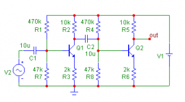
Well, I have learnt a lot here about feedback. To clarify, I have prepared the circuit (attached, working, I can encourage purists to build it). This circuit is built from two identical stages. Every of the stages has a gain of 5 (R2/R3 and R5/R6). Considered as single stages, they are feedback circuits. The feeback is constituted by R3 and/or R6. The gain of the stages depends only on resistor values when standard BJT device with h21e=300 or so used. But the amplifier as shown, created by cascaded connection of the two feedback stages is non-feedback or zero feedback. Great. I am finishing with this kind of discussion.
Attachments
Regarding that ultrafast no-delay transistor, this is a complete nonsense. As an example, emitter follower is happily oscillating circuit under some circumstances. Should there be no feedback it would hardly oscillate.
Charles Hansen said:When it comes to complete amplifiers, we have such luminaries as Nelson Pass, John Curl, and Scott Wurcer (designer of the AD797, AD711/12, and many more) agreeing that referring to an amplifier circuit as "no feedback" or "zero feedback" is the correct terminology to use when only local degeneration is employed. And that's good enough for me. I don't give a rat's *ss what Steve Eddy or Pavel say.
- Status
- Not open for further replies.
- Home
- Amplifiers
- Solid State
- Charles Hansen come in please