Hello.
Can you help me understand how to find this information in the datasheet ?
I read a lot of articles from different schools/uni but non of them explain how to find it, beside graphical approximation, and warn it's not precise.
I know that it is modulated by VDS but that's all.
I found out it's also called lambda and can be found in spice models, thanks to Elvee.
Thank you.
example : Channel Length Modulation in MOSFET (VLSI Design) – Buzztech
IF the datasheet happens to include curves of Ids versus Vds, you can extract the output conductance gds
gds = dIds / dVds
since it's the slope of the curve. Then write down your equation using channel length modulation and isolate gds on the right hand side. Plug in the numerical value of gds from the datasheet, and solve this equation for channel length modulation. Done!
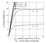
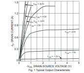
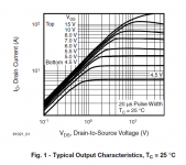
Here are two P-channel MOSFET graphs from two datasheets. Notice the sneaky way they denote negative voltages and negative currents.
_
gds = dIds / dVds
since it's the slope of the curve. Then write down your equation using channel length modulation and isolate gds on the right hand side. Plug in the numerical value of gds from the datasheet, and solve this equation for channel length modulation. Done!
Here are two P-channel MOSFET graphs from two datasheets. Notice the sneaky way they denote negative voltages and negative currents.
_
Attachments
Thank you guys. Yes I found out it's not explicitly in datasheets.
And some datasheets have completely flat curves at the saturation region (which seems they do not want you to determine 1/lambda).
Mark, when you talk about the slope, do you talk about the slope in the triode region (the initial slope) or the slope of the saturation region ?
Here page 24 they they explain the slope of the saturation region :
http://www-inst.eecs.berkeley.edu/~ee105/sp08/lectures/lecture16.pdf
To keep things confusing, power MOSFET designers usually call the saturation region the linear region and sometimes call the triode region the saturation region.
Thank you. I was confused because in the lecture16.pdf page 9 it said :
"Small gate length and oxide thickness yield low channel resistance, which will increase the drain current."
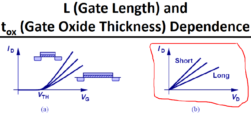
And page 24 added :
"For long L, the channel‐length modulation effect is less than that of short L."
At first, I tough to just use the "current" slope to determine, the effect of channel length modulation.
I thought, the higher the current for a vds, the lower the gate length, the lower the effect of the modulation.
But it's not reliable because the oxide thickness also affect the "current slope".
I know I may ask too much but can someone demonstrate the real world equation examples.
On how to find channel length modulation between 2 different mosfets, so I can can do it again after.
Because I am lost. Sorry.
"Small gate length and oxide thickness yield low channel resistance, which will increase the drain current."
And page 24 added :
"For long L, the channel‐length modulation effect is less than that of short L."
At first, I tough to just use the "current" slope to determine, the effect of channel length modulation.
I thought, the higher the current for a vds, the lower the gate length, the lower the effect of the modulation.
But it's not reliable because the oxide thickness also affect the "current slope".
I know I may ask too much but can someone demonstrate the real world equation examples.
On how to find channel length modulation between 2 different mosfets, so I can can do it again after.
Because I am lost. Sorry.
Last edited:
In your case (gyrator application), you do not need to delve into the gory details: what interests you is the output conductance, which is mainly dependent on lambda, which in turn depends on the geometry, etc, but basically you have two sources of information: the datasheet and the spice model.
Neither is always very complete or reliable regarding this information, because it does not matter a lot for switching applications.
In the DS, you simply have to look for the horizontality of the flat part of the Id/Vds characteristic:
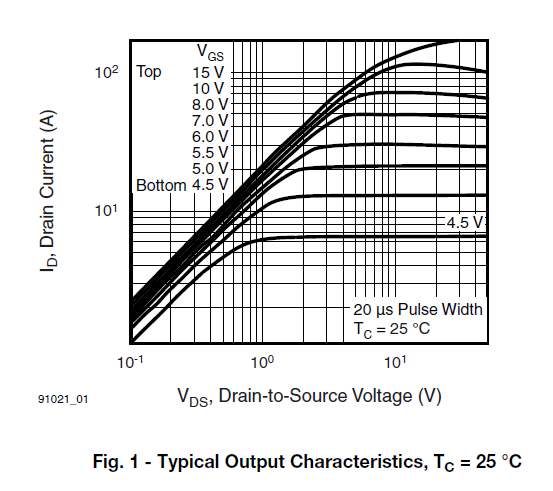
For this IRF540 example, the 4.5V curve looks perfectly horizontal, and that's one of the problems: the resolution provided by a normal graph is very crude compared to what you need to estimate kiloohms or tens of kiloohms.
With a spice sim, you can zoom in and evaluate tiny slopes, but the reliability is, let's say moderate...
The only reliable solution is to measure the PSRR yourself, after a first crude preselection based on the data available.
Note that measurements made on a type of MOS made by one brand are generally not going to be applicable to other brands, because this parameter is not essential for the applications of these devices
Neither is always very complete or reliable regarding this information, because it does not matter a lot for switching applications.
In the DS, you simply have to look for the horizontality of the flat part of the Id/Vds characteristic:
For this IRF540 example, the 4.5V curve looks perfectly horizontal, and that's one of the problems: the resolution provided by a normal graph is very crude compared to what you need to estimate kiloohms or tens of kiloohms.
With a spice sim, you can zoom in and evaluate tiny slopes, but the reliability is, let's say moderate...
The only reliable solution is to measure the PSRR yourself, after a first crude preselection based on the data available.
Note that measurements made on a type of MOS made by one brand are generally not going to be applicable to other brands, because this parameter is not essential for the applications of these devices
Attachments
Thank you guys I will do this, better buy 10 models and test them in real life.
There is no way to have enough information to make a reliable choice.
I will "trust" LTspice and see. Thanks to everyone.
There is no way to have enough information to make a reliable choice.
I will "trust" LTspice and see. Thanks to everyone.
Hi Federico, one quick piece of feedback. On the opening post (post #1) always state the WHY you are asking the information. Clearly Elvee knew the why (to build a gyrator) but the rest of us did not. Doing this will help you get better answers.
Ok, thank you I will keep this in mind.
I wanted to build a gyrator for a power supply to replace a CLC with a 16h choke.
Have a nice day and thank you all.
I wanted to build a gyrator for a power supply to replace a CLC with a 16h choke.
Have a nice day and thank you all.
- Home
- Amplifiers
- Solid State
- Channel‐Length Modulation in mosfet datasheet