as you know
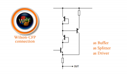
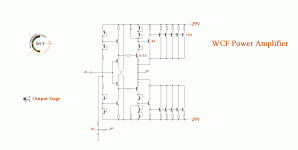
the Sziklai pair also known as a "complementary feedback pair" (CFP)
have a resistor
http://www.epanorama.net/sff/Misc/Amplifiers/Complementary_Feedback_Pair.pdf
my scheme drastically reduces the instability
Click on the diagram🙂
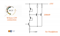
the Sziklai pair also known as a "complementary feedback pair" (CFP)
have a resistor
http://www.epanorama.net/sff/Misc/Amplifiers/Complementary_Feedback_Pair.pdf
my scheme drastically reduces the instability
Click on the diagram🙂
Attachments
That looks good. Does it have any affect on linearity -- distortion? And, also as a push-pull version?
-THx RNMarsh
-THx RNMarsh
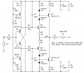
Assuming transistors Q2 and Q4 are identical (figure attached), Q2's current must be less than Q4's current. They have the same base voltage but Q2's emitter voltage is less than Q4's emitter voltage, due to the IR drop across R5. Thus Q2's base-to-emitter voltage is smaller than Q4's base-to-emitter voltage. Thus Q2's current is smaller than Q4's current.
Therefore "current booster" Q2, can only increase the total output current thru R6, by a factor of two at most - because Ic2 < Ie1. In my opinion, this nullifies one of the big advantages of the CFP, namely its enormous current gain (Iout / Iin). In a standard CFP the current gain is proportional to the square of Beta, while in this circuit the current gain is merely proportional to Beta. In fact it's less than 2 x Q1_Beta.
Therefore "current booster" Q2, can only increase the total output current thru R6, by a factor of two at most - because Ic2 < Ie1. In my opinion, this nullifies one of the big advantages of the CFP, namely its enormous current gain (Iout / Iin). In a standard CFP the current gain is proportional to the square of Beta, while in this circuit the current gain is merely proportional to Beta. In fact it's less than 2 x Q1_Beta.
Attachments
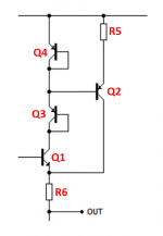
+1Assuming transistors Q2 and Q4 are identical (figure attached), Q2's current must be less than Q4's current. They have the same base voltage but Q2's emitter voltage is less than Q4's emitter voltage, due to the IR drop across R5. Thus Q2's base-to-emitter voltage is smaller than Q4's base-to-emitter voltage. Thus Q2's current is smaller than Q4's current.
Therefore "current booster" Q2, can only increase the total output current thru R6, by a factor of two at most - because Ic2 < Ie1. In my opinion, this nullifies one of the big advantages of the CFP, namely its enormous current gain (Iout / Iin). In a standard CFP the current gain is proportional to the square of Beta, while in this circuit the current gain is merely proportional to Beta. In fact it's less than 2 x Q1_Beta.
And why is the OUT where it is drawn 😕
Mona
I would assume that Q2 is a power device and Q4 is similar to a driver device.Mark Johnson said:Assuming transistors Q2 and Q4 are identical (figure attached)
And there was I always thinking that stability problems were caused by unwanted parasitic feedback, rather than current-voltage transformations. If this version of CFP is more stable, then this arises from the reduced internal gain - which may have to made up elsewhere.Stee said:The advantage is stability
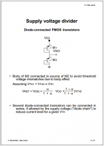
current don't need to transform itself in voltage and again in current
to control the unit gain
Roughly speaking, this is an emitter follower augmented by an asymetric current mirror. I am unclear what Q3 (in post 3) does - it will increase Miller effect in Q1.

Q3 (in post 3) cut RF on Q1
Stee, do you mean, it eliminates possible oscillation this way?
In this case, it's very interesting. I have to run some simulations 😉
Hi,
Q4´s dynamic resistance is lower than a discrete resistor at this position.
Should allow for higher bandwidth of the CFP and probabely less oscillation tendency.
I can´t follow Stee´s explanation for the function diode connected Q3 either.
First guess would go in the direction of some kind of temperature compensation, but certainly not for "cutting RF in half".
Your sure You didn´t simply drew a wrong connection and that Q2´s base belongs connected to Q3´s base instead and Q4 is a discrete Resistor? 😉
jauu
Calvin
diode chain
is the best method (as I know)
to have pure current coupling
it's works like a local voltage divider
that avoid critical threshold
white noise
so the RF oscillation
probably the cutting theory is NOT true: P
don't know if simulator can look this effect
is the best method (as I know)
to have pure current coupling
it's works like a local voltage divider
that avoid critical threshold
white noise
so the RF oscillation
probably the cutting theory is NOT true: P
don't know if simulator can look this effect
Attachments
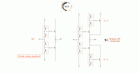
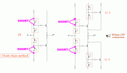
Does anything bad happen when I install short-circuits as shown in lavender color below?
It doesn't look like current mirror any more 😉
WITH short-circuits as shown
the noise increases
it becomes susceptible
for example, when you have gain in voltage
generates RF
this is the reason why no one uses the CFP (the SuperDevices)
the noise increases
it becomes susceptible
for example, when you have gain in voltage
generates RF
this is the reason why no one uses the CFP (the SuperDevices)
Hi,
in the marked circuits there's no current mirroring taking place.
Signal-in is fed into emitters and Signal-out is fed from emitters.
The 'outer' diodes also don't form current mirrors.
Stee, You are still just claiming effects but You don't explain the mechanism behind.
What is the secret noise draining mechanism of the diode connected transistors?
So far I only see that the diodes drop a bit of voltage and -beeing real life devices- generate noise.
Also, depending on the supply voltage rails the sourcing or sinking resistors may become considerably smaller in value.
This in turn may be positive for a CFP, as the base resistor of the slave transistor in a CFP should be small.
Could it be, that the nodes between the Diodes become low impedance nodes (emitter), which would be medium-to-high impedance without?
jauu
Calvin
- Status
- Not open for further replies.
- Home
- Amplifiers
- Solid State
- cfp - variant --> current coupled