Direct connect to PSU of these components string gives the same voltage drop - 14.7V\14.8V on zeners, 2K2 are little warm.
This is normal. Don't worry.
If VAS and CCS have no load, can they draw such current in the idle? I'm still confused because before the IPS worked with single 2K2 resistors.
They are not drawing any current until you connect all the input transistors. The heating is due to current flowing through the diodes and the parallel resistors from + rail to - rail, and a bit through the 100R feedback resistors to ground if the two CCS segments are installed.
I can't guess how it worked earlier. Can you upload a couple pictures of the first channel that worked?
Shaan, can I used 4K7 1W or 0.5W on the OPS instead of 2W types?
I am guessing you are talking about the two resistors feeding the two LEDs. With 50V supplies they dissipate about 0.5watt each. So using 1W is okay, but 0.5W may overheat.
How to determine optimal BE resistors value on the drivers, which currently 33R?
That depends on the load placed on the MJE15030/15031 transistors. Low load - higher value, high load - lower value. Looking at the huge O/P section with so many bases to drive, it is apparent that the load is high on these transistors. 33R seems like an adequate value.
Last edited:
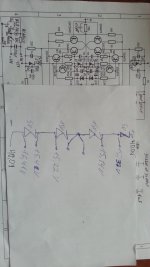
Yes, here is the picture. The difference were I used TL431 with paralleled resistors for them (25K, 5K) instead of zeners and a wire on top for GND connection between OPS and IPS. When I forgot to connect this GND wire and powered up the PCB I got this issue. Now this wire is permanently connected and goes under the PCB. I built second channel with the same TL431 chips but with other input transistors (from different supplier) than I used in first channel built - the results are the same as now - sag on 15V zeners, even 1V lower then on zeners.
Before when I powered the first PCB at first time I got 15V on all zeners as on the other picture. Later I found out this was due to an error - there was a mistake on silkscreen in the middle of input transistors and I confused npn-pnp of two pairs of input transistors. After the npn-pnp change the voltage on all zeners became correct - 5V and 15V. Than when I tried to set a higher bias current for the input transistors from 2mA to 3mA I forgot to connect mentioned GND wire and I got this issue with high DC offset 200-400mV and 6-7V on 15V TL431 and zeners.
Yes, I'm talking about these 4K7 resistors, I thought they are some kind of bleeder resistors. I'm not using the exact schematic I recently showed you. This one, basically the same but with 3 OP pairs, not 6, 35V\45V supplies, 2SC3423\2SA1360 on VAS, 2SC5171\2SA1930 as drivers and TTC5200\TTA1943 as output devices. So, perhaps 0.5-1W for 4K7 and 100R for BE on drivers should be Ok?
Attachments
![20170413_123926[1].jpg](/community/data/attachments/567/567424-3e0f5a48eb4531bf68fc7f021dbdba77.jpg?hash=Pg9aSOtFMb)
![20170407_151147[1].jpg](/community/data/attachments/567/567457-0350a7486fc02f61fe5dcc538d4525a1.jpg?hash=A1CnSG_AL2)
Last edited:
So, up to now the discussion has been on quite a different amplifier than your build. Keeping the participants (and those who were puzzling without actual participation) uninformed about your severe modifications is disrespectful at least, I'd say.
Best regards!
Best regards!
You are wrong Kay, I mentioned this before. You could check it in earlier posts. Just repeated it for Shaan. The previous schematic shown was aimed for SE IPS demonstration only, as the problem is in IPS section. No disrespect at all from me, only gratitude for help.
Last edited:
I don't see any information about the input segment mod we have been talking about. O/P segment discussions can wait for later don't worry. Let's get the input sorted out first, one step at a time.
Did you install the input transistors?
Is the problematic amplifier working now?
Did you install the input transistors?
Is the problematic amplifier working now?
Sorry, I wanted to try to find out what's drawing the current after I desoldered all 8 input transistors before install them back, it's very time consuming process. When I powered only zeners and resistors string, 2K2 resistors were relatively hot, when I'm trying the same in amplifier with CCS and VAS, 2K2 resistors are cold. So TO-126 transistors are drawing almost all the current (CCSs draw only for LEDs, top most CCS transistors are little warm). They (TO-126) have Vbe 0.6V and Vce 28V\30V. With all input transistors installed they had Vce 35V\36.5V.
Voltage drop on zeners in amplifier was 12.7V\13.15V with 85R on pots, 13.8V\14.2V with 100R on pots without input transistors.
Voltage drop on zeners in amplifier was 12.7V\13.15V with 85R on pots, 13.8V\14.2V with 100R on pots without input transistors.
Last edited:
When I installed all 8 input transistors, voltage on 15V zeners become 13.98V\14.34V with 100R on pots and 2K2 current set resistors. How it could be with even more load?
Tried with 550R 2W and all input transistors. First I had 500mV DC offset, when soldered CCS transistors directly to PCB I had 1.4V DC offset with 60R pots. When 80R pots DCoffset 0.5mV, with 70R pots - -90mV. Also there is a hiss noise from the speaker when DC offset on output. 550R 2W are little hot. Zeners voltages are ok. I noticed, after I power off the amp resistance on pots could be 5R different than I set them before with up to 10R difference between pots, than it comes closer to original values but not exactly as I set the resistance before powering up.
Last edited:
Shaan, with 12V 5W bulb on output the DC Offset is 20-25V, bulb glows. Is it normal such high offset?
Recently I found the problem of voltage drop on zeners. It was oscillations on 200MHz transistors (VAS and predrivers). I installed 33pF as per schematic and bulb on output extinct with 500R 2W current set and 65R on pots, DC offset was 0.5V. I changed 500R 2W current resistors to 750R 4W and voltage on zeners was the same, but when I touch by DMM lead to one 10R emitter resistor bulb glows, until I installed 22pF on VAS transistors. Than I raised the current on input transistors by setting the pots to 50R and bulb glows again, DC offset 1.8V; when I change 750R 4W to 1.5K 2W voltage on zeners become 12.5\13V and DC Offset only +100\-100mV. So, to raise the voltage on zeners I'm using second 1.5K 2W (or 2.2K, 10K) in parallel but getting DC offset as bulb glows and perhaps oscillation somewhere.
Last edited:
I built many CFP amplifier. I found that it good to add some series resistor at the input, even together with the low pass filter. It can oscillate without it.
I use 220ohm series, and 220pF parallel.
My amp is rock solid since I added this RC filter.
Sajti
I use 220ohm series, and 220pF parallel.
My amp is rock solid since I added this RC filter.
Sajti
I don't know why, perhaps wrong DMM reading, but on second check with 1.5K 2W current resistors DC offset 0.9V and dropping, Voltage drop on 15V zeners 14.5V
Recently I managed to remove dc offset to zero from the output, increase a current on input transistors up to 3mA. If push it more the amp suddenly starts to oscillate, I guess, as light bulb tester glows at full power coupled with like radio sigmal coming out from the speaker and 0.5V DC offset. The same happens on cold start with 3mA input transistors current setting.
Also there is still 0 - 0.2mV bias current on OP devices which is unable to increase with installed 500R pot. Perhaps should I increase 56R on the Vbe multiplier?
Everyone is welcome to express a thoughts.
Also there is still 0 - 0.2mV bias current on OP devices which is unable to increase with installed 500R pot. Perhaps should I increase 56R on the Vbe multiplier?
Everyone is welcome to express a thoughts.
Last edited:
Yes, Sorry, maybe it's not CFP but CFA amp. My mistake in the thread.
Do you mean 33R to some higher values like 100R?
Could the instability at >3mA input bias current be due to overload of TL431A? According to datasheet, max. Ika is 100mA at 2.5V, so, with 15V on TL431 max. Ika should be 16.7mA, but I have 30-32mA or 14.5-15.6V drop on current set 495R resistors.
Do you mean 33R to some higher values like 100R?
Could the instability at >3mA input bias current be due to overload of TL431A? According to datasheet, max. Ika is 100mA at 2.5V, so, with 15V on TL431 max. Ika should be 16.7mA, but I have 30-32mA or 14.5-15.6V drop on current set 495R resistors.
Last edited:
Vbe multiplier I'm using was designed for 6 OP pairs, I'm using 3 OP pairs, perhaps there is the problem?
Your predriver and driver ( MJE15031 and 2SC3788 ) are in CFP configuration.
Wonder why you used the TL431A. Jeez, you are in a spot of trouble. As suggested earlier by someone, simulate it in LT Spice or another Spice simulator and look at the voltages and currents. Compare it with what you have and see what's wrong.
Wonder why you used the TL431A. Jeez, you are in a spot of trouble. As suggested earlier by someone, simulate it in LT Spice or another Spice simulator and look at the voltages and currents. Compare it with what you have and see what's wrong.
TL431 are better than zener. It was recommended by designer LC as a preferable substitution of zeners. Where there could be a trouble using TL431? The only flaw I've observed in this schematic TL431 need little more current to operate than zeners.
I and Cortez who suggested me to simulate the schematic made it and he tried to simulate it but without success. All files are here a few pages earlier. I'm not familiar with simulation, I can't do this until someone shows how to do this correctly.
I and Cortez who suggested me to simulate the schematic made it and he tried to simulate it but without success. All files are here a few pages earlier. I'm not familiar with simulation, I can't do this until someone shows how to do this correctly.
Last edited:
- Status
- Not open for further replies.
- Home
- Amplifiers
- Solid State
- CFP Amplifier - Help Please!