The corner frequency of the R/C needs to be at a specific place; for this amp it's 1.5MHz. It depends on the Cbe of the drivers. If it causes ringing in your other amps, perhaps it needs retuned, or isn't actually needed. If your OPS is very fast, it may have an effect only at frequencies higher than would cause ringing.
To tune it I would use 220R for the resistor (careful about OPS bias) and sweep through capacitance to find the sweet spot, using group delay or small-signal square shape as my reference. Then halve R, double C, repeat, until you find the smallest R that will work.
To tune it I would use 220R for the resistor (careful about OPS bias) and sweep through capacitance to find the sweet spot, using group delay or small-signal square shape as my reference. Then halve R, double C, repeat, until you find the smallest R that will work.
To clarify, I was meaning 1mV matching between same parts, not complimentary.
With the transistors I got, matching complimentary devices would be hard because you couldn't do better than 1mV or so from normal, since the individual device spreads are so low. And if you DID manage to find one transistor in a large batch that had significantly different Vbe, how do we know that device wasn't damaged by ESD or is a dud?
Yes, between same devices it's easy to get very tight matching. But, between complements across batches you will get spreads and if the degen is very low - as in my case- there will be issues on volume builds due to spreads. This problem is exacerbated when all 4 input stage devices are not complements.
All part of the CFA learning curve . . .
Just ran into the same issue - had to tell builders to "up" the IP diamond Re's
to 39R ... I run 1.8-2ma at ip (70+mv Re). 🙁
Had overshoot and the servo worked too hard to correct offset.
Now, having both fully adjustable CCS's and the servo , I can
advise for even higher values for higher gain IP pairs.
My builders are throwing everything in the "junkbox" into my amps 😱 .
The amount of current feedback also affects the ease of mitigating
offset. So , One must compromise between slew , how large and how hot
your FB resistors have to be , and the ease in which the servo can correct
all this. (or , in your case ... the passive offset trim).
PS - I have also advised to match the IP P/N with a DMM , at least get "close".
OS
OS, yes 70 mV looks good. I've gone a bit higher at 120 to 150 mV
You could match the Vbe's as well, but I think this detracts from the ease of using bipolar devices - better just to make the design 'fool proof' which is what these higher degen voltages do.
IC guys don't have these Vbe hogging issues because they normally have a whole library of devices they can pick and choose from to optimize the diamond front end.
John, there is no reason for any added complexity in a cfa. It is just a matter of what some believe in, High open loop gain or high bandwidth ;-)My concern with CFA topologies is not the design of the input stage, as much as the ADDED COMPLEXITY of the second and output stages that seems to go along with most designs put up here.
In my world, less is best in serial, and more is OK in parallel.
About parallel and serial, i think we are living in the same world ;-)
IMV CFA 2nd stage and OPS complexity is no more than a VFA - you can make it simple or more complex - it really depends on the performance you are after. With a CFA a straight non buffered TIS/VAS (i.e. single transistor) stage +EF2 gets you to below 100ppm at full power at 20 kHz. Add complexity to move forward from there - a buffered VAS and EF3 and you are at single digit ppm. Almost all of the CFA designs show cased here are still single gain stage.
I would think a fully balanced JFET input stage + folded cascode are as or complex than the diamond buffer + VAS designs we are seeing on this thread though . . .
I would think a fully balanced JFET input stage + folded cascode are as or complex than the diamond buffer + VAS designs we are seeing on this thread though . . .
Bonsai,
Except for the point that OS's output stage in high powered I would have to say that the total circuit with the the Nad input section seem fairly simple. I am no wiz at building amps but this seems to be a straight forward build that most people can build. Unless you are looking for a Pass first watt how much simpler can it get?
Except for the point that OS's output stage in high powered I would have to say that the total circuit with the the Nad input section seem fairly simple. I am no wiz at building amps but this seems to be a straight forward build that most people can build. Unless you are looking for a Pass first watt how much simpler can it get?
OS, yes 70 mV looks good. I've gone a bit higher at 120 to 150 mV
You could match the Vbe's as well, but I think this detracts from the ease of using bipolar devices - better just to make the design 'fool proof' which is what these higher degen voltages do.
IC guys don't have these Vbe hogging issues because they normally have a whole library of devices they can pick and choose from to optimize the diamond front end.
Just go to dual devices for the diamond....
http://www.mouser.com/ds/2/302/PBSS4140DPN-50354.pdf
Or many other low Cob matched P/N smt's - most are $.50 each.
Perfect for a 1-2ma low voltage diamond...
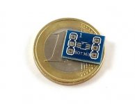
So as not to scare 😱 builders with SMT ...an adapter for through
hole(below) . 😀
OS
Attachments
Ah yes, I know those parts well . . . I get as many free samples as I need 😀
But I avoided them on the sx and nx because most folks are not happy with SMD - although personally I enjoy working with them down to SOT23, SOD100 etc. Below this it can get a bit difficult though.
But I avoided them on the sx and nx because most folks are not happy with SMD - although personally I enjoy working with them down to SOT23, SOD100 etc. Below this it can get a bit difficult though.
Bonsai,
Except for the point that OS's output stage in high powered I would have to say that the total circuit with the the Nad input section seem fairly simple. I am no wiz at building amps but this seems to be a straight forward build that most people can build. Unless you are looking for a Pass first watt how much simpler can it get?
Agree!
Ah yes, I know those parts well . . . I get as many free samples as I need 😀
But I avoided them on the sx and nx because most folks are not happy with SMD - although personally I enjoy working with them down to SOT23, SOD100 etc. Below this it can get a bit difficult though.
I didn't mean for the builder to do it. 😉
I wish you could send a few free samples to my builder... (Thimios).
He'd print it out (below - adaptor) in seconds .
Easy to make a custom dual ECB / EBC to 363 adapter for drop-in
compatibility. 😀
OS
Attachments

Bonsai,
Except for the point that OS's output stage in high powered I would have to say that the total circuit with the the Nad input section seem fairly simple. I am no wiz at building amps but this seems to be a straight forward build that most people can build. Unless you are looking for a Pass first watt how much simpler can it get?
VSSA simple .... 4 device 😀 . Amazing. 😎
OS
I didn't mean for the builder to do it. 😉
I wish you could send a few free samples to my builder... (Thimios).
He'd print it out (below - adaptor) in seconds .
Easy to make a custom dual ECB / EBC to 363 adapter for drop-in
compatibility. 😀
OS
Could be a nice avatar for somebody 😀
Why ? Is an electronic device to be designed for the builder's comfort or the best results (shorter is better) ?most folks are not happy with SMD
Christophe,
I'm not sure that my eyes are good enough anymore to work with surface mount devices, even with magnification, but I would be willing to give it a try. Do you think that the actual end result would be perceptibly better with some surface mounts devices and the shorter path lengths, I imagine that we would still be using the same output devices for the final output section? Good to see you in this thread, have you been watching the Slewmaster thread, some very nice designs have been presented there.
I'm not sure that my eyes are good enough anymore to work with surface mount devices, even with magnification, but I would be willing to give it a try. Do you think that the actual end result would be perceptibly better with some surface mounts devices and the shorter path lengths, I imagine that we would still be using the same output devices for the final output section? Good to see you in this thread, have you been watching the Slewmaster thread, some very nice designs have been presented there.
Why ? Is an electronic device to be designed for the builder's comfort or the best results (shorter is better) ?
Purely related to eyesight and fine motor skills issues. It also takes practice and good technique.
😎
As I see it, SMD is for the manufacturer not for the home DIY builder. The thing that will decide is IF semiconductor makers will stop making thru hole parts, (which they have already started) and then those of poor eyesight will invest in microscopes and push these tiny parts around a board and HOPE and PRAY that they stick. My first try with the Wurcer preamp was ghastly messy with solder flux making an unsightly mess. Ray
Thanks, Kindhornman, for your nice words. Yes, i think so, SMD can provide visible benefits both on the bandwidth and the stability margin. Not to forget that with CFAs, we can deal with 10MHz issues. Of coarse, we have to learn and change our habits to use them. Not so difficult with accurate tools and methods, in fact.Do you think that the actual end result would be perceptibly better with some surface mounts devices and the shorter path lengths, I imagine that we would still be using the same output devices for the final output section?
And, yes, i had looks at the the Slewmaster thread. The problem is the same than here: How to figure how valuable some ideas can be when you're interested mainly in listening results and some contributors are so aggressive each time some want to enter in this 'subjective' world ?
I' had experimented a lot of combinations in the past, Diamonds, Cascodes, buffers, CCS etc... And i'm sure of one thing, you cannot rely on sim results, specially harmonic distortion numbers to figure out what can bring this or that. The only way i believe in is to start with the simplest design you can, and validate each added complexity only after careful comparative listening sessions. And, often, the conclusion stay the old one: "Simple is beautiful".
Last edited:
To do SMD to a high standard you absolutely require:-
A FINE tipped 30 W soldering iron
FINE tipped tweezers
1 mm diameter solder
Good eyesight, or alternatively good specs
Access to the dozens of Youtube videos showing you how to do it
It is easy, fun, and can confer performance benefits.
A FINE tipped 30 W soldering iron
FINE tipped tweezers
1 mm diameter solder
Good eyesight, or alternatively good specs
Access to the dozens of Youtube videos showing you how to do it
It is easy, fun, and can confer performance benefits.
Bonsai and Christophe,
Perhaps someone can take one of the two designs of OS and convert the design to surface mount and produce a PCB that can be used to assemble the end product? It would be interesting in a side by side test of the surface mount and the thru hole to see if this can be heard. That would follow with Christophe's request for listening tests and not just sim results.
When I say one of OS's designs I am talking about the NAD1.3 version and the Symisim design I believe.
- Home
- Amplifiers
- Solid State
- CFA Topology Audio Amplifiers