Re offset/bias.
Be warned that if the degeneration voltage applied to the front end devices is too low, you will get problems.
About 60 (30 sets) individual nx-Amp boards have been sold and I've had 4 complaints where the output offset could not be dialed out and or the second stage bias was wrong (this is tested by measuring the voltage across the 1 k collector load resistors of the diamond buffer output stage).
In the original design, I used 15 ohm resistors and 1 mA standing currents to generate 15 mV degeneration.
This is not enough to deal with the normal Vbe spreads, and you can end up with some amps where the diamond output stage is starved of current and/or the aforementioned offset issues. HFE matching by the way will NOT solve the problem - it's a delta Vbe issue between the transistors.
To overcome this, I raised the degen voltage to 150 mV and 120 mV for the buffer and level shifter respectively by changing the 15 Ohm resistors for 150 Ohms and 110 Ohms.
The offset adjustment is now smooth and gives +-500 mV range, and the standing current variation spread from unit to unit will be much narrower.
There is an errata sheet posted up in my website, and I've added it to the sx & nx amp thread.
To be sure, if you use complements for the input stage (so BC557C and BC547C for example) and a cascode, the problem will be much reduced, but I would still encourage the use of higher degeneration voltages on diamond buffers. In the nx-Amp, I've used a 45 V Vce BC5x7C for the buffer, and 65 V Vce rated BC5x6B for the level shifter because I did not want to use a cascode and it seems this also contributed to the now solved problem.
On one full builds, problems like this would likely not be caught - you'd build and get away with it as was my case where I built 2 protos, and then two final boards with no issue, only discovering the problem after building a further two. When you produce many exemplars, spread issues like this will raise their heads.
I spent a few hours testing and pushing the two new boards this week end and am extremely happy with the results. Square wave 100 kHz at near full power and rise fall times of c 700 ns - so no change to the performance.
I think that you are wrong here. If you keep the same current trough transistors than how you can meliorate DC offset by changing emitter resistor, Vbe (NPN-PNP) difference will show independent of the values of those resistors. In my opinion only by Vbe matching it's possible to lover DC offset.(or use DC servo)
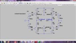
Here is a simulation, I used Andy_C models as I think they are quite accurate.
Did I get it all wrong?
BR Damir
Attachments
Those are Cordell's models. Andy's models have the A suffix.
All offset here is cause by Hfe which is matched only at one current. Changing degeneration changed the current, so the Hfe is no longer matched, producing different offsets across the 30k resistors.
I don't see this as a good representation of an input stage currently in use however, it would be more accurate to have the 30k resistors in series with the ground lead to the base voltage sources.
Those are Cordell's models. Andy's models have the A suffix.
All offset here is cause by Hfe which is matched only at one current. Changing degeneration changed the current, so the Hfe is no longer matched, producing different offsets across the 30k resistors.
I don't see this as a good representation of an input stage currently in use however, it would be more accurate to have the 30k resistors in series with the ground lead to the base voltage sources.
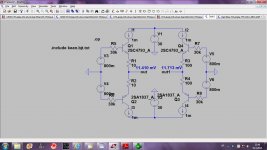
There are the CCS defining the currents, so degeneration does not change the current.
Here is simulation with Andy_C models, my bad I was thinking that _C meand Andy_C.
Attachments
Oops.
And oh my, you're saturating the transistors from the outset with current sources into the collectors!? Check Vce for all transistors.
And oh my, you're saturating the transistors from the outset with current sources into the collectors!? Check Vce for all transistors.
What is changed between Andy_C and Cordell models ?
When simulating , I do notice slight variations in operating points-saturation
-group delay ... etc.
Is any group of these models better than the others ?
PS- at least they ARE better than OEM models (realistic).
OS
When simulating , I do notice slight variations in operating points-saturation
-group delay ... etc.
Is any group of these models better than the others ?
PS- at least they ARE better than OEM models (realistic).
OS
Thanks for posting this up.
I've just redone my sims. For gain stepped from 10dB through 31.5 dB the -3dB CLG moves from ~575 kHz to 350 kHz with the ~575 kHz remaining essentially constant from 10 dB through 25 dB CLG which I would equate with the gain sweet spot often referred to in CFA application notes. This is with the bridge tie resistor set to 100 Ohms.
With the tie resistor set to 10 Ohms the -3 dB CLG drops from 575 kHz to 520 kHz over the same range. I would conclude that the BW is independent of the gain with these results.
If I MC the amp, then I get classic VFA behavior. At the low gain range end the -3 dB is at 530 kHz while at 31 dB CLG the -3 dB BW is 155 kHz
. . . )
😎🙂
from somewhere on the coast near Central America ...
Last edited:
Andy_C got very good Hfe and Ft accuracy among other things, I don't remember how well Cordell did. I think Andy was more detailed, he used spreadsheets and optimizer programs, so I'd trust his models more.
The actual device dies may have changed since Andy made his models, so they may not be quite the same. OnSemi came out with a lot of different versions of these devices since Andy made his first models. The differences are probably not large enough to be a big problem.
The actual device dies may have changed since Andy made his models, so they may not be quite the same. OnSemi came out with a lot of different versions of these devices since Andy made his first models. The differences are probably not large enough to be a big problem.
I think that you are wrong here. If you keep the same current trough transistors than how you can meliorate DC offset by changing emitter resistor, Vbe (NPN-PNP) difference will show independent of the values of those resistors. In my opinion only by Vbe matching it's possible to lover DC offset.(or use DC servo)
Here is a simulation, I used Andy_C models as I think they are quite accurate.
Did I get it all wrong?
BR Damir
Dadod,
The degen resistors on the front buffer pair raise the base voltages of the second set of transistors. That means the emitters of the second pair are further apart voltage wise. To maintain the same collector current, you therefore have to increase the second pair degeneration resistors.
This can be confirmed by measuring the volt drop across the degeneration resistors.
The idea here is that the higher degeneration voltages are now 8-10x the probable Vbe deltas between the transistors and are therefore much more manageable i.e. 120 to 150 mV in my case. This then allows any offsets to be trimmed out. Importantly, current hogging/starving is now also only a fraction of what it is with low degen voltages - 5 to 10 %.
If you are using a servo, it would disguise the problem - however, I am sure on a AP test, distortion would be high because the second stage bias would be affected (current hogging or starving) - so even with a servo, you really need to solve the root cause of this issue by providing higher degen voltages.
hFE matching while useful, will not solve the problem if you use low degen voltages of 10-20 mV. In that case you will need to match Vbe's.
Last edited:
😎🙂
from somewhere on the coast near Central America ...
Happy Hols. From a smoggy Beijing!
Dadod,
The degen resistors on the front buffer pair raise the base voltages of the second set of transistors. That means the emitters of the second pair are further apart voltage wise. To maintain the same collector current, you therefore have to increase the second pair degeneration resistors.
This can be confirmed by measuring the volt drop across the degeneration resistors.
The idea here is that the higher degeneration voltages are now 8-10x the probable Vbe deltas between the transistors and are therefore much more manageable i.e. 120 to 150 mV in my case. This then allows any offsets to be trimmed out. Importantly, current hogging/starving is now also only a fraction of what it is with low degen voltages - 5 to 10 %.
If you are using a servo, it would disguise the problem - however, I am sure on a AP test, distortion would be high because the second stage bias would be affected (current hogging or starving) - so even with a servo, you really need to solve the root cause of this issue by providing higher degen voltages.
hFE matching while useful, will not solve the problem if you use low degen voltages of 10-20 mV. In that case you will need to match Vbe's.
Yes, as I said on your thread http://www.diyaudio.com/forums/solid-state/236522-sx-amp-nx-amp-74.html#post3823774.
But, I still do not like diamond buffer. Can someone suggest better solution?
The diamond buffer is a very good circuit Bimo.
It's just a fact of life that with discrete implementations you have to either match the Vbe s or use other techniques like increased degeneration to deal with the issue - IC designers have much more control over these parameters.
However, raising the degeneration voltages as described above solves the issue. And, in discrete form (read: audio power amplifiers and line stages) and in IC form (CFA input stages and output buffers) there are many hundreds of millions of circuits all working reliably and without issue.
Da larger emitter degen resistors reduce i/p Gm and also introduce noise.The degen resistors on the front buffer pair raise the base voltages of the second set of transistors. That means the emitters of the second pair are further apart voltage wise. To maintain the same collector current, you therefore have to increase the second pair degeneration resistors. ...
... loadsa good stuff on how to make evil Diamond inputs behave 😱
I'm claiming this as a win for simple CFA like VSSA & what I posted in #822 etc 🙂
You need a servo or twiddle pot for both evil Diamond & simple.
The disadvantage of course is needing big evil electrolytics. 😱
But I have a supply of electrolytics handcarved by virgins from solid Unobtainium which have vanishing levels of THD, supa musicality bla bla.
Send me $450 in used bank notes and I'll send you a sample. You won't be disappointed.
.. but seriously folks .. I'm looking at one of Guru David Zan's applications which needs 1nV/rtHz noise at the i/p and zillion W o/p so that precludes evil Diamond i/p.
As I pointed out earlier, simple CFA is a Classic Very Low Noise topology.
______________
I actually have an active ribbon mike application which requires matched Vbe. Can't figure out how to do even a simple trim without introducing noise. Things are difficult below 1nV/rtHz
Last edited:
The diamond buffer is a very good circuit Bimo.
It's just a fact of life that with discrete implementations you have to either match the Vbe s or use other techniques like increased degeneration to deal with the issue - IC designers have much more control over these parameters.
However, raising the degeneration voltages as described above solves the issue. And, in discrete form (read: audio power amplifiers and line stages) and in IC form (CFA input stages and output buffers) there are many hundreds of millions of circuits all working reliably and without issue.
I still learning and still do not confident to try diamond buffer. I am playing with simple VSSA input and try to optimize it.
Of the choice between the two (VSSA / diamond 2 stage) ,
I chose the 2 stage diamond input.
Those "evil" VSSA caps increase LF THD .. even as they do mitigate
offset . Great for a low power amp...but, I like <1mv - period.
The 2 stage (nx) can be tweaked to low double digit ppm. As far as
cost and layout ... almost equal (servo vs. caps - tl072 is cheep !)
Also with the 2 stage you can use 40V low Ic precision devices for
the diamond and "harden" the 2'nd stage with to-92L High voltage-high Ic devices.
The 2 stage has an even better solution ... use a quality op-amp as first
stage (instead of the diamond) and a discrete higher Ic/Vce 2nd stage ...
Wait till you see the "next" CFA !!!
OS
Dadod,
The degen resistors on the front buffer pair raise the base voltages of the second set of transistors. That means the emitters of the second pair are further apart voltage wise. To maintain the same collector current, you therefore have to increase the second pair degeneration resistors.
This can be confirmed by measuring the volt drop across the degeneration resistors.
The idea here is that the higher degeneration voltages are now 8-10x the probable Vbe deltas between the transistors and are therefore much more manageable i.e. 120 to 150 mV in my case. This then allows any offsets to be trimmed out. Importantly, current hogging/starving is now also only a fraction of what it is with low degen voltages - 5 to 10 %.
If you are using a servo, it would disguise the problem - however, I am sure on a AP test, distortion would be high because the second stage bias would be affected (current hogging or starving) - so even with a servo, you really need to solve the root cause of this issue by providing higher degen voltages.
hFE matching while useful, will not solve the problem if you use low degen voltages of 10-20 mV. In that case you will need to match Vbe's.
Bonsai, I understand all that, but what I am trying to say is that you can't decrease DC offset caused by Vbe mismatch with degeneration increase. When I said you need matching I meant Vbe matching ( to some degree, and the rest DC servo will do) not hfe.
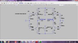
I am not sure that my simulation is the best representation of this. Here I matched the base currents and transistors are out of saturation.
Attachments
I'm claiming this as a win for simple CFA like VSSA & what I posted in #822 etc 🙂
Clear win, also soundwise.

I actually have an active ribbon mike application which requires matched Vbe. Can't figure out how to do even a simple trim without introducing noise. Things are difficult below 1nV/rtHz
Trim Vbe by temperature? You can change temperature by varying Vce to change dissipation. This works about just as well when coupled face to face, so external temperature modulation would be minimized.
What a brilliant idea! 🙂Trim Vbe by temperature? You can change temperature by varying Vce to change dissipation. This works about just as well when coupled face to face, so external temperature modulation would be minimized.
Will have to reduce temperature as I don't want to increase kTB. I've done some stuff for cryogenic transducers.
Might as well take advantage of this and operate the whole thing at 1 degree Kelvin 😀
Da larger emitter degen resistors reduce i/p Gm and also introduce noise.
I'm claiming this as a win for simple CFA like VSSA & what I posted in #822 etc 🙂
You need a servo or twiddle pot for both evil Diamond & simple.
The disadvantage of course is needing big evil electrolytics. 😱
But I have a supply of electrolytics handcarved by virgins from solid Unobtainium which have vanishing levels of THD, supa musicality bla bla.
Send me $450 in used bank notes and I'll send you a sample. You won't be disappointed.
.. but seriously folks .. I'm looking at one of Guru David Zan's applications which needs 1nV/rtHz noise at the i/p and zillion W o/p so that precludes evil Diamond i/p.
As I pointed out earlier, simple CFA is a Classic Very Low Noise topology.
______________
I actually have an active ribbon mike application which requires matched Vbe. Can't figure out how to do even a simple trim without introducing noise. Things are difficult below 1nV/rtHz
I ll settle for the virgins only thanks, now how much are those ?? 450$

Dont claim a win so fast. Its easy to get around this problem. Members here just havent found the correct solution. Look at Nad, Myryad, Cyrus, Accuphase and others, do you see them having this problem ?? No
Do they rely on SMD closely matched pairs ?? No.
This is for John Curl too. I wonder if he knows that the recently released products from Ayre which is getting high accolades in the audio press are CFB designs, and all feature the dreaded Diamond buffer. I mention John as I believe he respects Charles work. See what Charles Hansen says about the diamond (Hifi News Oct 2013). Dont if you dont like the diamond 😀
Clear win, also soundwise.
Obviously you havent listened to a krell, accuphase Myryad, Arye and even low cost Cyrus models. Nothing wrong with the diamond. Your ears are lying to you, fortuneatly others know better. 😀
- Home
- Amplifiers
- Solid State
- CFA Topology Audio Amplifiers