The high slew rate being achieved in the CFA designs is an interesting matter.
Cheers,
Bob
I repeat what I said before, there is a BIG difference between taking a bag of parts and having the freedom to attack a fixed problem in several ways and making general purpose blocks where the user has limited choice of external components and no choice of internal ones.
The H bridge input amp is a good example. The discrete designer has choice via the 5 resistors to independently set input bias current and transconductance. I don't think it is too much of a stretch to say that one can achieve the same GBW and slew rate as a CFA with a given feedback R and because there is ONE closed-loop gain target the Ccomp can be chosen for optimum closed-loop BW. The resulting VFA (IMHO) will probably have better PSRR and CMRR by simple symmetry and a very comparible error budget with respect to THD due to output stage errors. I think this arguement is moot in several respects.
No offense taken at all, but I hope you don't take offense by me pointing out again that the input to a so called CFA circuit in situ is not between the plus and minus pins on a so called black box but from the plus input to ground through the feedback network, i.e. the voltage across the plus and minus pins is not the input the current flowing caused by this voltage is. This current charges the comp cap and makes the voltage at the gain node.
EDIT - I would hope we can stay out of being offended one way or the other and just have a friendly arguement.
Of course you are right, but then we (or at least me) do not talk specifically about op amps, I did not say "CFAs are VFA op amps...". An op amp is a particular kind of "black box" (or a particular case of a 2 port, or di-port, used in feedback theory). For those interested, here's the way of using Thevenin and Norton theorems to convert and analyze in an unified way such circuits. EE 101.
The high slew rate being achieved in the CFA designs is an interesting matter. Besides the so-called current-on-demand action, there is obviously the issue of how the feedback is compensated.
Take a look at the compensation OS used in his excellent design. I would argue that it is a form of Miller Input Compensation (MIC). I achieved 300V/us with MIC in my 50-watt MOSFET power amplifier. So I don't think high slew rate is exclusive to the realm of CFAs.
Cheers,
Bob
Thank you on feedback resistor comment.
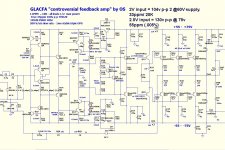
I would apreciate if you comment the compensation I used hare, http://www.diyaudio.com/forums/solid-state/243481-200w-mosfet-cfa-amp-43.html#post3753533
It is a kind of OIC (output included compensation) and I could achieve with it quite high slew rate and exellent phase and gain margin.
BR Damir
The high slew rate being achieved in the CFA designs is an interesting matter. Besides the so-called current-on-demand action, there is obviously the issue of how the feedback is compensated.
Take a look at the compensation OS used in his excellent design. I would argue that it is a form of Miller Input Compensation (MIC). I achieved 300V/us with MIC in my 50-watt MOSFET power amplifier. So I don't think high slew rate is exclusive to the realm of CFAs.
Cheers,
Bob
Thank you , Bob.
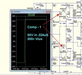
Comp. 1 below is standard (luxman does this on the M120a).
Not bad , but not a "slewmaster" 😀 .
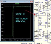
Comp. 2 below is the MIC . wow!
I have done the "housekeeping" on the design (last attachment). In simulation ,
I can not find any issues. In fact , none of my sims have a greater
model/passive component tolerance.
I scaled to 75V rails and "pushed it" . Slewed from rail/rail (-6V) in .2uS ! (with MIC).
PS - Bonsai recommended MIC to me - credit where it's due !
OS
Attachments
Last edited:
Hi Esperado, so, should we give up on the one recording which has no op-amps in favor of the many which do?It is not this, Jay. Please think about the following:
Apart some rare classical recordings, done with two mikes strait in the mastering machine, the only 'transparent' reproduction system for a given record is the one witch was used during mixing session. As dirty as it was.
wouldn't it be nice to enjoy the occasional recording as it was recorded?
design for the few rather than the many.
Thank you , Bob.
Comp. 1 below is standard (luxman does this on the M120a).
Not bad , but not a "slewmaster" 😀 .
Comp. 2 below is the MIC . wow!
I have done the "housekeeping" on the design (last attachment). In simulation ,
I can not find any issues. In fact , none of my sims have a greater
model/passive component tolerance.
I scaled to 75V rails and "pushed it" . Slewed from rail/rail (-6V) in .2uS ! (with MIC).
PS - Bonsai recommended MIC to me - credit where it's due !
OS
Os,
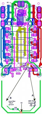
From where the decision to connect the feedback shunt resistor to main audio ground and not to input signal ground?
Os,
From where the decision to connect the feedback shunt resistor to main audio ground and not to input signal ground?
That is the question I asked Mr. Marsh.
Actually, "G2" is the secondary star connected to the high current
main star (G1). This was Andrew T's idea and serves well in reality.
What I noticed with CF ... If I connect to the lifted ground "behind"
the 10R resistor ,the 50ma currents from C4 modulate that ground.
On the NX or a typical VFA (less current) , this will only take a few PPM
off of the THD.
On the VSSA , I hooked it's 2 caps to the lifted ground and THD
suffered considerably. Unless I get an answer , I might just have
a jumper to connect to either ground on the prototype.
OS
So, if i understand well, OPAs are bad because they are not hype ?design for the few rather than the many.
Hi OS,
50mA in itself shouldn't be a problem. The question is how much of this current is distorted.
Cheers. E.
50mA in itself shouldn't be a problem. The question is how much of this current is distorted.
Cheers. E.
Last edited:
So, could we apply the feed back to the emitter of a LTP and thus have the best of both worlds?Huh? Did I say a CFA has poorer PSRR? I only said that the common diamond buffer input stage has a lower PSRR than the long tail pair input stage.
So, could we apply the feed back to the emitter of a LTP and thus have the best of both worlds?
I have no idea how you could do that. The common emitter connection of a LTP is a virtual ground, so that would not work.
Is there a way the MIC-compensation can be applied to the stripped down version (no diamond front end) but split resistorfeedback VSSA front end..??
Member
Joined 2009
Paid Member
You can provide connections to both base-inputs of an LTP and also the common emitters. I did this with my very first amp, TGM(1) and it's also in my TGM6 (Pioneer). But it isn't always good for low distortion - try reading about Gilbert mixer cells !
Is there a way the MIC-compensation can be applied to the stripped down version (no diamond front end) but split resistorfeedback VSSA front end..??
I tried Soooo hard .... I was not bright enough to succeed. 😱
OS
Happily, the peak/average power ratio in music and resistance's thermal inertias are high enough.
I would not make that conclusion without testing its assumption at a reasonable - sustained - high average output from a 100-200W PA. Better for the time being to use more than enough Wattage (non smd) at this part in the fb circuit.... that is what I would do. Going to very low values is probably (assumption) not needed if, as was pointed out, the noise reduction and SR are at a point where it becomes impractical to have a very large wattage resistor. That makes good common sense to me.
BUT... if you wanted to go crazy on the design and didn't care about such practical matters and go for lowest noise, thd, IM, highest Sr, Bw etc that is humanly possible without regard to annoying things like cost and size.... it sure would be interesting and I would like to hear it.
Thx-RNMarsh
Last edited:
Where to tie the fb resistor and the input resistor.... The input R is also the terminating R for the preamp OPS loop. The current thru this input R is sourced and returned to the preamp. Not withstanding any leakage** from input of PA. So that loop needs to be isolated/separated from the preamp PS and the PA PS grounds and not get 'mixed' together or over-lapped. An area which the PCB layout artist expertise is needed.
** topologies which reduce the input (modulated) 'leakage' or devices (cascoded jFETs) that do so will help with distortion reduction due to the reduction in potential mixing at the fb/input area.
Thx-RNMarsh
** topologies which reduce the input (modulated) 'leakage' or devices (cascoded jFETs) that do so will help with distortion reduction due to the reduction in potential mixing at the fb/input area.
Thx-RNMarsh
Last edited:
You can provide connections to both base-inputs of an LTP and also the common emitters. I did this with my very first amp, TGM(1) and it's also in my TGM6 (Pioneer). But it isn't always good for low distortion - try reading about Gilbert mixer cells !
Schematic?
I've heard of the Gilbert cell 😀, and I don't see how it applies here. The Gilbert cell core functionality has nothing to do with audio amplifier applications.
P.S. Never mind, I got it. That's common mode feedback, designed to increase the VCC PSRR of the pnp diff pair input stage. Has nothing to do with setting the closed loop gain, current feedback, etc... and it is used as a cheap way to compensate for the missing active current source feeding the LTP. Making the Pioneer a cheap design.
Last edited:
So it's not just me being dumb, as I can't get MIC to work, but I can make Cherry work, that improves distortion figures more than 10 times, so you have less than 10 PPM at full throttle 20 kHz
Last edited:
No 🙂So it's not just me being dumb
But, if all those various compensation schemes can give better distortion numbers, did-you notice any difference in listening ?
Where to tie the fb resistor and the input resistor.... The input R is also the terminating R for the preamp OPS loop. The current thru this input R is sourced and returned to the preamp. Not withstanding any leakage** from input of PA. So that loop needs to be isolated/separated from the preamp PS and the PA PS grounds and not get 'mixed' together or over-lapped. An area which the PCB layout artist expertise is needed.
** topologies which reduce the input (modulated) 'leakage' or devices (cascoded jFETs) that do so will help with distortion reduction due to the reduction in potential mixing at the fb/input area.
Thx-RNMarsh
I'll try the visualization method of communication.
Below is the ground scheme , I use this for VFA , but I tie the "drawn"
R-C to the lifted ground. Both NFB and G2 will be wires bridging the PCB.
OS
Attachments
- Home
- Amplifiers
- Solid State
- CFA Topology Audio Amplifiers