In simulation, 100mv in gives 10v out! Gain of 100. Is it only me or does anyone else think this is an awful lot of gain? I believe CFB amps are somewhat different to VFB amps in this regard, but still...😱
Let me answer the question with a question. The schematic depicts two floating batteries/supplies, each with 39 Volts DC. Assume that you have no other additional power supplies / DC sources.What do you mean by peak to peak output swing limitations? Can you tell me more?
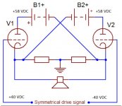
What is the maximum signal swing on the speaker, that can be achieved in the circlotron configuration?
Circlotron - Wikipedia
How about the traditional approach? Will taking the alternative route, with the "traditional" architecture, with -39, 0, +39 VDC, symmetrical rails and speaker referenced to ground, promise a higher? similar? lower? value of the maximum possible theoretical output signal voltage swing? Will the two architectures, using the same supplies, provide you with similar output power?
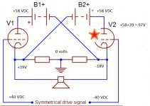
I am trying to imagine a driver pushing one of the circlotron gates with +38V relative ground. The other (symmetrical) driver pushing the other gate with -38V. What will happen?
I have my views on this, but I dare not say them out loud. Not sure.
Tell me how you see this.
In the middle of the circlotron's 4+4 ohm speaker, you have your ground reference.
In the case of the traditional architecture, the 8 ohm speaker has one of the ends grounded.
In the circlotron: what is the maximum voltage peak that can be achieved on one of the ends of the speaker, when compared NOT to the midpoint, but to the OTHER end of the speaker?
I have abandoned my circlotron diy project mid-ways and now I am "restructuring it" so as to converge to the traditional architecture with symmetrical rails.
Last edited:
I shall ask 🙂 as I can't seem to produce a PDF myself with anything like the fine resolution of the one that was sent to me earlier... unless there is some secret to doing it.
Thanks😀 I could have kissed our IT guy when he put me on to a great little free virtual PDF printer called CutePDF. At the time we were editing house plans for architects (we did the audio / video and automation) using Autocad. A0/A1 paper is huge! We used professional printers. To access the drawing you need Autocad and our printers lost their copy of the software. Huge drama...until I found I could print to this 'virtual' printer from my software, any software. Problem solved. It works great with Spice too.
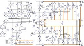
One notable difference between the simulation and the hardware is the use of LT1056A for op.amp use rather in the simulation in lieu of LME49860. The former has a JFET input the latter has BJT input.
U4 and U3 have ac coupling between the output and the inverting input. It may be worth simulating with a suitable BJT input op.amp to see if there is a problem with the choice.
The layout of this circuit would have to be critical requiring due attention to decoupling of the supplies to high performance op.amps. This should be done close to the op.amp voltage supply pins. The associated resistor values suggest high circuit impedances.
In the real hardware C34 and C36 which decouple the supply pins are only 5.6nF which looks highly suspect. That raises the question if the 7815 and 7915 regulators are adequately decoupled as well.
Last edited:
I'm sorry to read that you are abandoning your Circlotron project 🙁 Before you do, please consider starting a thread and posting your ideas and the schematic. To me this is a most interesting and unusual technology, and I suspect also for many others on this forum.Let me answer the question with a question. <snip>
To answer your question, or at least part of it, just off the top of my head, I expect the Circlotron output depicted here to go to the supply rails 39-0-39 less the base emitter drops of the output devices and also the driver. In this instance about 78v - 1.2 - 1.2. There will probably be some other losses I have not allowed for but I did drive it to clipping in the sim and got more or less what I expected. I must stress that I am not an amplifier designer so probably not really qualified to answer your question anyway. I am slowly working my way through some great books by Douglas Self and Bob Cordell (may they live forever) and hope to improve my knowledge this way. But it is not so easy for me. Maybe something to do with teaching old dogs new tricks? 🙂
But I am sure you have your reasons for asking. What do you dare not say? I for one would be interested to hear.
You know we probably have our own ways of understanding electron flow (and lets not forget those mysterious minority carriers, the holes which dare to go in the opposite direction no doubt just to confuse us) so I read with interest all your questions ending 'with reference to what?' and for me I don't get hung up on it because for me 'ground' is a relative thing. If an NPN transistor has its base grounded 'ground', no problem, you can still switch it on. Simply make the emitter more negative than ground and the device turns on. Where the electrons come from I don't care, as long as they get the job done 🙂 So in the case of the -43V rail for the bias, that’s fine by me. (But still odd).
Beware: this is a fast and dirty, preliminary and untested, un-simulated draft version of what was on my mind, .... before i abandoned it (in essence, not even sure if it would work):I'm sorry to read that you are abandoning your Circlotron project 🙁 Before you do, please consider starting a thread and posting your ideas and the schematic. ...
Electron tube front end;
Short signal path;
AC coupling (beginners mode - coupling capacitors - allows to treat front end and back end somewhat separately);
Fully symmetrical forward paths;
Fully symmetrical negative feedback paths;
Thermally stable Sziklai based OPS, without need for thermal compensation;
OPS batteries: 4x floating 58V DC, 10 Amps; 0.2F filter.
Brutal Force electron tube pre-driver;
Non-standard driver, Sziklai "master" with negative temperature coefficient
Paralleled "slaves" with "irrelevant" temperature coefficient;
Driver and Output transistors screwed directly (no electrical insulation) on to the copper speaker bus-bars, via silver paste (such as for microprocessors). Speaker bus-bars electrically insulated from heat sink. Contact area between each bus-bar and heat sink: 4cm x 38cm;
4 x 0,3K/W heatsinks;
2 x toroidal 1,1kW, 2x 43VAC, 12A.
Current gearbox ratio between Sziklai master and slaves ensures isothermal stability
Speaker terminals mounted to the (extruding) copper bus-bars, rather than to the chassis.
Manual KISS bias for upper and lower branch;
Simple two-slope WAG current limiting; Red LED's signal that a current limiter kicked in;
{edit: some battery symbols need be rotated}
... Abandoned due to unsatisfying peak-to-peak output swing capability.
{edit: the picture as presented - has single slope current limiters}
So here is a riddle:What do you mean by peak to peak output swing limitations? Can you tell me more?
Heavy input swing: +/- 40V.
Assuming 1V saturation of ordinary BJT transistors (not tubes), what is the output voltage on the speaker terminals?
What Vce voltage rating for the BJT transistors?
Attachments
Beware: this is a fast and dirty, preliminary and untested, un-simulated draft version of what was on my mind, <snip>
What a fascinating looking circuit. I would like to try and draw it out in Spice to try and understand it better one day. It certainly looks like you went to a great deal of trouble and expense with your prototype - but you say 'untested', so there was no prototype? So how would you know there was insufficient p-p swing? Funny you should mention leaving out the insulators on the heatsink. Bose do (or did) that with some of their products. Since anodizing is non conductive, if done properly, you can treat your metal anodized heatsink as an insulator. I think 'done properly' are the operative words here 🙂
So here is a riddle:
Heavy input swing: +/- 40V.
Assuming 1V saturation of ordinary BJT transistors (not tubes), what is the output voltage on the speaker terminals?
What Vce voltage rating for the BJT transistors?
It is indeed a riddle. So you have drawn essentially the output stage in the Spice model on this thread. For each tube we substitute a NPN transistor with the collectors to the positive supplies and emitters to the load. I see you have included your virtual ground (over and above the invisible midpoint of the load) which the Spice model does not have. And I should say the answer is 78v but in reality it is zero? Did I pass? 🙂 Now my head is hurting so I think I will open a packet of chips and watch a movie 🙂
A different variation of this circuit, went it's separate ways, and is now being produced by another guy. There was a time when this idea was discussed between the two of us. We still talk to each other. Theoretically. Anyways, he went for the low output power, rich standing current, single mosfet pair, cap coupled to a single pair of triodes within a duo-triode bulb. Long Tail Differential Pair, and .... that was about it. Not even sure if he had enough open loop bandwidth to close a feedback loop around it. It works. It sells.
...
I am under the impression that you misunderstood my remark about the speaker-bus-heatsinks. The output transistors, together with the 2sk1058 lateral mosfet "driver transistor", are purposefully galvanically connected to the speaker-bus-heatsinks. Via conductive silver paste. It was intended to take special care to ENSURE that there is a good electrical connection between the source of the 2sk1058 and the collectors of the 2sa to the speaker bus heatsinks. Take a look at the schematic again. The brown lines are bus bars. Two of them are pre-heatsinks. HOT.
It is the speaker-bus-bar-pre-heatsinks (copper: 42cm x 4cm x 0,5cm) that are electrically insulated from the heat sink proper.
Agreed, the speaker output terminals, those mounted to the speaker-bus-bar-heatsinks, will be hot. Who cares? As long as they do not melt - let the music play.
Wiki has drawn it. I just borrowed the graphic and put on some voltages. Yes, the tubes are simply NPN transistors. Plus from batteries to the collectors, Minuses to the speaker and emitters. The "virtual" ground is ... very real. It is your reference point for the voltages that control the bases of the transistors. It is in the middle of two half-speakers.It is indeed a riddle. So you have drawn essentially the output stage in the Spice model on this thread. For each tube we substitute a NPN transistor with the collectors to the positive supplies and emitters to the load. I see you have included your virtual ground (over and above the invisible midpoint of the load) which the Spice model does not have. And I should say the answer is 78v but in reality it is zero? Did I pass? 🙂 Now my head is hurting so I think I will open a packet of chips and watch a movie 🙂
The question now is: how do you get 78 Volts on the full speaker, if the battery has only 58V? Assuming that one of the transistor bases "sees" +40V signal. It would be logical to assume that the emitter and associated half-speaker "sees" +39V. But referenced to what? To the other end of the speaker? NO !!!!
{ Archimedes: Give me a place to stand, and I shall move the world. }
It is referenced to the speaker midpoint. Now, since the speaker is actually a series connection of two logical four ohm speakers .... +39 ... 0 ... that would imply, that on the "other end" of the full speaker you have -39V. But .... Where is it supposed to come from?
Such a voltage is not available. Such a voltage does not exist. The battery has only 58 Volts. You can not get 78Volts from a 58 volt battery. What about the "other battery"? It does not help whatsoever. It is passive and is not doing anything. Apart from trying to fry the other idling transistor, stressing its Vce_max.
Maybe I am wrong in this thinking, but that is how I "see it".
Last edited:
OK, I'm probably too darned slow here, but gotta jump in -- this thing has had my brain all bent up for days.
syn08 (post #3) and mjona (post #7) lanced and dispatched several excellent points. But there are some other bits worth mentioning IMHO.
The diamond buffer has several issues. Operating both sections at the same current density (R37=R17==R68=R69) gains little and exaggerates transistor imbalances. I'd rather see a 5 - 8:1 increase from the first pair to the second. Also, the 'normal' output node (the joint between R68 and R69) cannot be driven as you would the inverting input of an op amp -- it needs a return path to ground. Without it we won't get the current unbalancing to the current-mirrors that we want. And it needs to stay within about +/-25 mV of the input -- the Bases of Q24 and Q28 -- so it is useful for global NFB. Just lift the op amp (U2, U3) ends of R45 and R47 and connect them to signal ground for each side. Gotta admit the compound drive is beautiful aesthetically; but what nightmare headaches can come from giving that stiff pair of emitters so much influence over U2/U3's outputs!
The current-mirror topology also needs some work -- 48:1 is too high of a current gain ratio. Try lowering it to 6 or 10:1 by replacing the 2k4 resistors R53 and R72 with 330R or 470R. Then give the diamond buffer more current by lowering R38 and R39, and let the 2nd stage have more of it by increasing R37 and R17. (Formulae for this are available, but I don't have them handy. Probably faster/easier to just tweak them in LTSpice, anyway.)
I haven't seen a cascode VAS yet that didn't have stability 'problems'. The doubled Q5/Q20 and Q21/Q22 are especially puzzling to me -- it can't be for dissipation concerns since the Vce is about 5V. More parts means a wider distribution of specs -- and much higher sensitivity to device variability. The Darlington only compounds your troubles. I'd remove them and select higher gain devices for Q5 and Q22. If you simply must keep them, add a forward-biased 1N4148 or similar between the Base and Collector of Q40 and Q27. That'll fix the unmatched # of Vbe's, restoring linearity and temp stability.
Even with these changes transistor selection will be crucial -- you can probably forget rolling part numbers. There may be only a few dozen devices in the whole book that will work without careful, tedious hand selection. There are plenty of good reasons that current mirrors are ubiquitous in analog IC designs; almost every one adds another challenge/shortcoming to a discrete design.
From the MJE1503x drivers (Q10/Q16) on, the problems get worse. These are current sources without a rational, resistive load -- the gain approaches infinity. C3 and C1 impart a 90 degree phase lag, adding another challenge to stability. Q1 and Q30 have no Base-Emitter resistor -- there must be one. Without it quiescent leakage alone can start thermal runaway, especially since this modest 2W device (the 2SCR375P at least) is tasked with driving 96A/1200W-worth of outputs. There is no temperature compensation or mechanism to control cross-conduction. The Collector currents of Q1 and Q30 have only the 390 ohm R20 and R79 to provide a return path to the bi-polar supply; the entire output stage -- both sections and their floating power supplies -- is/are pulled positive by those currents. The global NFB will then try to keep both outputs near bi-polar ground by the only means it has: Reducing the conduction angle which will dramatically increase crossover distortion.
Mooly , I think you were on to something by subbing FET's for Q1/Q30 -- solves the 'missing return path for their Base currents' problem. But it would be an increase from the (already problematic) 2 Vbe offset between Q10/Q16, and Q32/Q33 and the corresponding output pins.
Q13 is under rated. Even with R121 disconnected and no signal, Q13 is being asked to dissipate 1.42 watts. Even if it was capable of providing bias control, a more complex circuit would be required. I'd rather see R20 and R79 returned to bi-polar ground (someone else already suggested) -- that would allow good quality NFB without having to use an instrumentation amp topology or other sophisticated (read 'slow') techniques.
The existing input buffers would allow asymmetric signals in the output sections, which could cause problems. Much safer to convert the Balanced inputs to SE, then phase-split back to Balanced for the VAS. And yes, it is surely much uglier.
Take out one of the offset servos, U1 or U4. Having two just invites them to fight each other, making the result half as accurate. What we care about is the quiescent voltage across the speaker. The voltage between either terminal and bi-polar ground -- not so much.
It's a very aesthetically pleasing design, I agree. But I'm sorry, I don't think it will work -- IMHO.
Best Regards,
Rick
Thanks Rick, I can see you've put some serious thought into all this. I'll have to have a good read of it all tomorrow 🙂
Just to say though that it is all still very much 'ongoing' as we try to find a workable solution for it.
Just to say though that it is all still very much 'ongoing' as we try to find a workable solution for it.
One very real practical issue in all of this is that the amp is apparently very difficult to work on and that has slowed things down quite a lot, however some significant (very significant) improvement has come from increasing the value of the four 470pF caps (C1 and C3 that you mentioned) in the driver stage. Although partly disassembled at this point, the amp has seemed stable and could not be provoked into breaking into oscillation. Just adding 100pF to these seems to effect a 'cure', at least with the amp in bits.
I guess if we were looking at this as a 'design in progress' then there are many things that could be looked at to improve the repeat-ability of the build, in this instance though the tech working on this has to take it all at face value in that it is what it is.
The servo's looked strange from the word go, not so much the configuration but the choice of component values and not using FET opamps. That has been another area of investigation.
OK -- glad you've found something that helps.
And thanks for the help adjusting my perspective. I certainly do tend to get carried away at times ..😉
Cheers
And thanks for the help adjusting my perspective. I certainly do tend to get carried away at times ..😉
Cheers
One very real practical issue in all of this is that the amp is apparently very difficult to work on and that has slowed things down quite a lot, however some significant (very significant) improvement has come from increasing the value of the four 470pF caps (C1 and C3 that you mentioned) in the driver stage. Although partly disassembled at this point, the amp has seemed stable and could not be provoked into breaking into oscillation. Just adding 100pF to these seems to effect a 'cure', at least with the amp in bits.
I guess if we were looking at this as a 'design in progress' then there are many things that could be looked at to improve the repeat-ability of the build, in this instance though the tech working on this has to take it all at face value in that it is what it is.
The servo's looked strange from the word go, not so much the configuration but the choice of component values and not using FET opamps. That has been another area of investigation.
On the physical aspects of the problem, op.amps including the 7815/7915 regulators decoupling of the supply rails needs to be done properly in the interests of device nfb and stability.
The .asc file does not show any output leg decoupling capacitors for the regs, so is this an oversight?
If not the reg stability rests on the op.amp supply decoupling capacitors of a mere 5n6F.
With more that one dual package these caps would not be equidistant from the regulators and variations in the parasitic elements in the supply traces to each package would exist.
Thanks mjona, those 5n6's did get questioned and apparently the diagram as drawn is correct... so yes, a possible other issue. I think some extra decoupling was added as a test.
Another issue that the tech working on it found was that the 79 regulator wasn't regulating correctly (the voltage was high at nearly -17v) and this was blamed on the current draw of the opamps being so low as to be outside the minimum load requirement of the reg. Easy fix for that one of course.
It's one of those that the more you look... the more you see 😉
Thanks mjona, those 5n6's did get questioned and apparently the diagram as drawn is correct... so yes, a possible other issue. I think some extra decoupling was added as a test.
Another issue that the tech working on it found was that the 79 regulator wasn't regulating correctly (the voltage was high at nearly -17v) and this was blamed on the current draw of the opamps being so low as to be outside the minimum load requirement of the reg. Easy fix for that one of course.
It's one of those that the more you look... the more you see 😉
That is the trouble we cannot see, and unfortunately from the explanation given by the technician, he has to be kidding. I can guess what his fix was however the problem has not gone away - time to look at some basics to see if anything has been overlooked.
Take it or leave it a 7915 needs local decoupling capacitors on the input if this is more than 3'' (75m.m.) away from the negative supply capacitor i.e. a 2.2 uF solid tantalum or 25 uF aluminium.
In either case the output needs 1uF solid tantalum or 25uF aluminium. This is according to the National Semiconductor Linear Databook Volume 1.
A quote from the National Semiconductor Audio Handbook is that because of their high gain bandwidth, high impedance characteristics, IC's tend to be less forgiving of improper layout than their discrete counterparts. Many excellent ''paper circuits" wind up not worth ... and are needlessly abandoned in frustration."
Two points made in this piece are don't use IC sockets and pay due attention to supply decoupling.
- Home
- Amplifiers
- Solid State
- CFA Class A Circlotron with stability issues. Thoughts invited.