Still there!
Hi ilimzn,
due to lots of work still struggling through your posts in the CD63 mod thread.....
asolutely interesting!!!
Deep respect to your knowledge and your disposition to share this!!!
Will be back soon with a new post.
Have of course still a few 🙂 questions. Most regarding LED shunts and grounding issues....
Regards Ernst
Good Evening Ilimzn,
I have used 2 good (at least they should be, because we use the same at work) 1:10 probes, when I measured the clock signal. First signal really was a perfect sine wave. :-(???? No square!
I've seen clocks with a cap at the output, I thought about implementing one as well.
I fully agree.
Wow, what a thread 🙄 Found a pic of your spareplayer CD1020. Looks nice!! Just had a look, which DAC your Sony has. Would habe been happy, if it were a V24+ box, but wasn't. I have got an old SCD XB940 (too many inductors for you) laying around which is waiting for some mods. Accidently yesterday I found some really good info about how to get out the best of its DAC here in the forum in a very short thread. Will have a lot of work and fun with this player as well, but this is another and further away story....
Btw, one thing the 940 shares with the Marantz players are the groundloops. I'll look after them in both.

I also found this an many more in the thread, you mentioned. Probably this is the longest thread, I've ever seen. Never knew, that these players were/are soooooooo popular.
I found the description of your grounding approach (extremly interesting - for other projects as well, like amps aso), your using the original transformer approach (clock voltage should be connected to analog windings), your way of using existing pcb layout for your modification. You mentioned a few elder opamps, that should sound very nice in this particular circuits. You mentioned also, that I could use my HDAMs. Would you recommend using just the last HDAM stage and replace the other ones with opamps or do you think, they are ok in these positions as well?
Since I got so much info, I'll start this project by this or the next weekend. Step by step. Devil is in details, questions will be raised.
Cheers Ernst
Before deciding, be certain to check again with a 1:10 probe. A 1:1 probe has high capacitance and will round the edges of a square wave - the actual signals may have a much better form than you think.
The XIN pin on the SM5872 has lower tresholds than others and is the input to an inverting amplifier that drives the XOUT pin and the internal clock logic inside the SM5872. It does to an extent pay off not
to overdrive this pin, the datasheet also states it can be capacitively coupled to center the signal around tresholds.
I have used 2 good (at least they should be, because we use the same at work) 1:10 probes, when I measured the clock signal. First signal really was a perfect sine wave. :-(???? No square!
I've seen clocks with a cap at the output, I thought about implementing one as well.
This XIN/XOUT arrangement might present you with a 'built in' inverter for the clock, if you need one. You could conect the external XO to the XIN inputs of the SM5872, and use one of the XOUT outputs as the
clock output to the separation chip. In any case, mind that you give the best possible clock quality to the DAC chips themselves.
I fully agree.
I only loosely documented this mod, but there is actually a partial thread here about it, IIRC in the CD63 mod thread - search for Marantz CD1020. I will look up the relevant partial schematics and post them
as soon as I find them (probably tomorrow when I am close to the PC they are on).
My main player is a SOny CDP-X707ES, and the Marantz is my spare, but it does sound good - definitely light years away from the stock version. BTW there are a number of things no-one seems to get to in doing
CD63 mods - like ground loops on the board, and double analog and digital GND connections instead of in one single point.
Wow, what a thread 🙄 Found a pic of your spareplayer CD1020. Looks nice!! Just had a look, which DAC your Sony has. Would habe been happy, if it were a V24+ box, but wasn't. I have got an old SCD XB940 (too many inductors for you) laying around which is waiting for some mods. Accidently yesterday I found some really good info about how to get out the best of its DAC here in the forum in a very short thread. Will have a lot of work and fun with this player as well, but this is another and further away story....
Btw, one thing the 940 shares with the Marantz players are the groundloops. I'll look after them in both.
I do know how to set up a TL431 shunt, but to be honest, even after heavy digging I still do not know how to set up a LED shunt, as you proposed. Would you mind describing this a bit more in detail?To be perfectly honest, complex active devices with feedback - which would describe most high-tech regulators - present very complex impedances which also might end up misbehaving in the MHz region, which the SM5872 gladly spews out of it's power and grond pins, like most bitstream DACs. So, it comes down to simplicity. You only need a few mA from these supplies and the best experience which I had so far were
LEDs appropriately in series to get the right voltages. The dynamic impedance of a LED string is not terribly low - perhaps 10-20 ohms at currents between 10 and 20mA - but it is VERY stable, up to the
several tens of MHz. Also, because it is not very low and it's not resonant or inductive and only very slightly capacitive, it will not interact with any capacitors in parallel. So, you can concentrate on
choosing good caps or combinations of caps (caps with zobels etc...) which is actually much simpler than doing a well behaved active shunt. Just keep in mind not to use high efficiency LEDs, they tend to
have a bit higher impedance.
Second alternative sounds not to complicated, but still very good! I would certainly try a tube approach, if you sent a sketch, as you mentioned. Since this was my initially plan. But I'll try the silicone way first! Seems to be easier and I want to hear, what is possible with both techniques.- attenuate the output at the DAC. As usual, attenutaion followed by amplification results in a higher noise floor, as there are components whose noise does not get attenuated but it does get amplified.
- attenuate the output of the tube stage. This will normally have the form of a divider incorporated into anode resistors of the tube diff stage. It has the advantage of lowering output impedance, and if any
added noise is generated by the curcuit, it is also attenuated. It also keeps the system feedback-free if this is important to you.
- use feedback. The diff amp becomes similar to a differential arrangement of anode followers, and looks similar to Nelson Pass' supersymetry circuits. The output impedance is lowered, tube tolerances
mitigated by feedback, BUT it is difficult to balance the frequency characteristics of the diff amp sides if only one output is used (coupling caps introduce low frequency poles and zeros). Also, important,
at power up, the high anode voltage (before tubes heat up) can leak back into the DAC through the feedback and destroy the chip, so you need to take measures against it (protection diodes etc).
I already noticed, since you had made me looking more precisely at the circuits, but of course I didn't know about the disadvantage.You will notice that in your player they actually use parts of the filter as a divider to lower the voltage. This is not an ideal situation as it introduces a DC bias to the current out of the DAC, but only
from AVdd to AGND. This results in asymetrical rise and fall times from the DAC output stage affecting it's linearity. Fortunately, in your case I believe it can be avoided because of the differential use of
the DAC. As I said, it's very odd to me that they just basically did several copies of the basically CD63 circuits, instead of taking advantage of the actual topology.
Yes, they did. Actually there is no inductor.If it's the same as the CD63 approach, because of the relatively low PWM fundamental frequency, the output filter had to use a relatively low corner frequency which means it slightly infringes into the top
of the audio band. In the CD63 they used an LC correction network to mittigate this. As you may expect, I do not like the use of any cored inductor anywhere, and preferably no inductor at all, and they used
a low cost one that looks like a resistor. Using the propper diff to se converter, it is not necesary. I don't see it in the schematics you posted, though, but I have not analyzed and simulated the filter to
check it's passband, as time is short. Hopefully they use a better approach.
Thanks for thisA few words about this filter arrangement:
The DAC AOUT+ and AOUT- are actually the LO and LON, RO and RON pins respectively - as only one filter channel is shown. As I mentioned before, the first stage of the filter is differentially connected to
keep the HF on the output of the DAC chip confined inside a vary small current loop adjecent to the DAC.
The 100k resistors from OPamp + inputs to GND adjust the output level so that the output is approx. 2Vrms.
The first two OPamps form a buffer, which also introduces a small amount of amplification at the very top of the audio band, in order to compensate for the 0.25dB roll-off at 20kHz introduced by the passive
filter stages. The 39k/100p combo acts as a shelving filter which is counteracted at higher frequencies (above audio band) by the 100pF caps in the feedback path of the OPamps. The result is that the roll-
off at 20k is very small, below 0.1dB. Tweaking the 39k resistor (between 36 and 47k) rises and lowers the response producing about +-0.15dB around flat response at 20k. You may adjust this to taste, the
differences are subtle but unmistakeable. These two OPamps serve to present exactly the same load impedance for the passive filter network - 100k.
The final OPamp is a differential to single ended converter, also rolled off by the 220p caps. The different impedances presented by the + and - differential inputs to this circuit no longer present a
problem at this point because the passive filter signals are already buffered here.
The JFET with jumper is used to force the OPamp outpit into class A, when the jumper is installed - the JFET acts as a current sink.
The two pairs of outputs present on the CD1020 (the regular CD43/53/63 have only one) are used as DC and AC coupled outputs. The reason for this is that the mod alowes for changeing of OPamps, so depending
on the type used some DC offset may result. In reality it always ended up being up to about 5mV which should not make problems - I've used this with a fully DC coupled amp.
The purpose fot he mod, amongst other things, was to be able to evaluate different OPamps, so sockets were provided (using separate pins installed directly into the PCB for absolutely shortest signal path
and best signal integrity). Generally, the best results were obtained with FET input OPamps in the first stage and a bipolar input OPamp as the final amp.
In your case, the requirements differ somewhat.
For starters, the HDAM module can be configured to perform the role of the final OPamp - it is configured similairly in stock form.
Since your player has one 2-channel DAC per output channel, the first stage passive filter resistors (2x6.8k) will be connected differently.
In the simplest form, there are actually two DAC AOUT+ and DAC AOUT- points in your player. These would be LO, RON and RO, LON respectively. each pair should connect to the differential 150p cap by it's own
resistor with a vaule of 2x6.8k = 13.4k. In this way the outputs are resistively added keeping the equivalent impedance to the differential 150p cap the same.
A better solution would be to scale the filter components for even lower impedance values because connecting two pairs of DAC outputs to form one differential pair gives us the ability to source twice the
current from the DAC. Actual standard resistor and cap values will not permit a simple halving of resistors and doubling of caps (unless you really want to use a pair of resistors and caps in parallel for
each of the passive filter caps and resistors as shown in the schematic), so you must compromise some - and in the direction of higher than half resistor values. Say, scale the 150p caps into 270p, and scale
all the resistors by multiplying with 150/270. The lowering of impedances will lower noise generated by input current noise from bipolar input OPamps if such are used in the first stage. Not lowering the
impedances to their minimum values alowes the DAC to work into a higher apparent load per output pin, improving it's linearity, while retaining the virtues of lower input impedances as seen from the OPamp
inputs.
Increasing the caps is particulairly beneficial should you ultimately install a tube output stage - as it's miller capacitance will then appear that much smaller compared to filter capacitances, and that
much less impact the filter characteristic.
In case you decide to use a tube output stage, you can sonstruct is a true diff amp (as I discussed earlyer), in which case it can replace all of the OPamp circuitry. I will try to do a quick schematic of
the idea (including how to implemet the shelving filter compensation ofor HF droop) as soon as I have some time.
I also found this an many more in the thread, you mentioned. Probably this is the longest thread, I've ever seen. Never knew, that these players were/are soooooooo popular.
I found the description of your grounding approach (extremly interesting - for other projects as well, like amps aso), your using the original transformer approach (clock voltage should be connected to analog windings), your way of using existing pcb layout for your modification. You mentioned a few elder opamps, that should sound very nice in this particular circuits. You mentioned also, that I could use my HDAMs. Would you recommend using just the last HDAM stage and replace the other ones with opamps or do you think, they are ok in these positions as well?
Since I got so much info, I'll start this project by this or the next weekend. Step by step. Devil is in details, questions will be raised.
Cheers Ernst
Good Evening Ilimzn,
I have used 2 good (at least they should be, because we use the same at work) 1:10 probes, when I measured the clock signal. First signal really was a perfect sine wave. :-(???? No square!
I've seen clocks with a cap at the output, I thought about implementing one as well.
This pin is the output of the oscilaltor amp (XOUT) filtered by the crystal. As you know, the crystal is a very high Q resonator, which essentially means a very narrow band filter - so the sine you are seeing should be perfect as it is the 'overloaded' output (distorted signal) after all other frequencies excet the one the crystal is for, have been removed - so, a near perfect sine-wave.
Wow, what a thread 🙄 Found a pic of your spareplayer CD1020. Looks nice!! Just had a look, which DAC your Sony has. Would habe been happy, if it were a V24+ box, but wasn't.
No, it's just a regular CD player (red book). It does, however, use one of the best pulse DACs ever made. It's output gets within fractions of a dB of theoretical 16-bit performance with 16-bit input. It is a 20-bit DAC. You should hovever note that DACs that have truly 20-bit performance are very rare even amongst so-called 24-bit DACs.
I do know how to set up a TL431 shunt, but to be honest, even after heavy digging I still do not know how to set up a LED shunt, as you proposed. Would you mind describing this a bit more in detail?
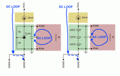
See attached pic below. Any element that has near-constant (ideally completely constant) voltage drop across it regardless of current through it can be used as a shunt element. That being said, in the real world, most of the effect is provided by a good capacitor accross it, while the semicondustor or vacuum shunt regulator provides the DC level.
In the pic attached, there are 2 versions of simple shunt regulation, the left one is with the TL431 shunt regulator chip, the right one with a series of LEDs. Keep in mind that actual component values are just representative, so in the real application should be tailored to the actual application - in particular the current source, and the capacitor(s). As drawn, the TL431 is set to 5V and the LED chain is 2x red and one IR LED, approximately 5.2V or so at the given current.
There are 3 parts to each verison, denoted by colored rectangles.
The reddish part is the actual load of the regulator, i.e. DAC, clock, OP-amp etc, which also includes it's own load (filter network, clock network, actual amplifier, respectively).
The green part is the shunt element itself - the one keeping th DC voltage constant regardless of current. In actuality, this action is not perfect, so voltage changes with the current, but the changes are very attenuated - in essence, it exhibits very low dynamic impedance. Also, a minimum and maximum current limit exists for each real element.
The yellowish part is the current source. In it's simplest form it can be a simple Idss connected JFET (gate to source directly conencted, and selected by resulting current according to need). A small damping resistor or even feritte bead inductor in series is a good idea to prevent HF coupling through the parasitic capacitance of the current source. The current source passes the same current regardless of the voltage across it, in theory. In actuality, the current varies very little with voltage changes. In essence, it exhibits very high dynamic impedance. Again, a minimum and maximum operating voltage exist for actual current sources.
Although it is not apaprent if one would look just at the schematics, this combination of elements forming a complete shunt regulator, is capable of separating the DC and AC current loops for the load and power supply.
Because the shunt element exhibits (idally vanishingly) low dynamic impedance, and is across the power supply pins that power whatever is supplying the signal to the load, so any load current has to appear across these pins as well, and current always passes through the path of least impedance, it will have to pass through the shunt element. Because 'dynamic impedance' literally means AC impedance, and these elements work to practically DC, all load current only stays withing the AC current loop as marked on the schematic.
In turn, because the current source is a very high dynamic impedance, any AC currents will not pass around the DC loop, which includes the actual power supply, pre regulation (Between AVcc and AGND). Of course, in reality, the current splits between the AC and DC current loops so there is always a residual of the AC current inside the DC current loop, but this residual is only as much as the ratio of dynamic impedances of the current source versus shunt element - the first being on the order of hundreds of kohms, and the second on the order of a few milliohms to a few ohms. So, the residual is a greatly attenuated version of the actual load current, or any current that appears between AVdd and AVss - easily 4-5 orders of magnitude if good layout and design is used.
It could be said that the DC current loop which is defined by the current source, only initially charges the capacitor in the shunt element until the semiconductor part limits the voltage on it. From there on, current is circulating around in the AC current loop, with the DC current loop only covering losses.
A non-obvious aside is that AC will not pass along a common path needed to connect all ground points, i.e. AGND and DGND, even if they are ultimately conencted to the same non-regulated power supply, and even if there are multiple paths. In reality, of course, the AC component will be strongly attenuated. (See dotted line in the DC current loop arrow). This means that if there is a common path for varius current returns, because the AC components in them are strongly attenuated, they have that much less chance to interfere with one-another and leak into power domains where they do not belong. The fact that they are creating a constant voltage drop (DC) across various ground paths is of little consequence as actual signals of interest are dynamic, and not static (of course, as long as voltage drops do not become excessive but then the device would not operate correctly in any sense anyway so this would be a fault rather than an imperfection).
Finally, most series regulators do not have this advantage, as they require some sort of capacitor at the input, which then connects the unregulated input via cap to the ground, alowing AC current from the unregulated input (due to ripple or nosie) into the local ground and from there along a ground return path to the unregulated source. In other words, now you gat an AC voltage drop along this path - or paths, which means that the ground reference will not be the same along the path, which in turn means that this AC component is in some amunt or form injected into various places in the circuit where it does not belong.
That being said, there are regulators that avoid this - the LM317/337 is one common example, but you have ti apply them carefully in this fashion. however, the concept is much more esily explained on shunt regulators as from the standpont of the unregulated supply, they look like a DC current sink, i.e. a two-pin element.
Second alternative sounds not to complicated, but still very good! I would certainly try a tube approach, if you sent a sketch, as you mentioned. Since this was my initially plan. But I'll try the silicone way first! Seems to be easier and I want to hear, what is possible with both techniques.
...
You mentioned a few elder opamps, that should sound very nice in this particular circuits. You mentioned also, that I could use my HDAMs. Would you recommend using just the last HDAM stage and replace the other ones with opamps or do you think, they are ok in these positions as well?
It's a bit unclear to me if you have the CD6000 or CD6000SE (se or balanced out). The schematic i put up is actually easily converted to a fully balanced output by addition of one more OP-amp or HDAM module.
Regarding tubes, it is actually easyer to do a simple balanced tube output than an unbalanced one, if the input to it is a balanced signal. For an unbalanced (se) output you need to implement a fully balanced circuit with both sides used as an output, but you take only one signal from one output, while you put a terminating ipedance equal to the output load on the unused outut of the tube stage. If that cannot be done, the tube stage gets more complicated as it needs followers on the output. The reason is that the load on the the output of the simple version needs to be equal on both sides or conencted between the outputs in order to equally infuluence both halves of the circuit, in particular the gain. If teh output load can be unbalanced, it has to be 'isolated' from the diff amplifier so that it does not influence it's operation, which complicates the circuit.
Attachments
Last edited:
Ilimzn,
Thank you for the LED shunt circuit and description!!
My player output is single ended, and adjacent equipment is SE as well. So the rebuilt player should be SE again. The circuit you posted - with the three opamps - seems to be perfect for me. My player has got three HDAMs per channel. In the pic I added, you can see circuit of CD6000. Instead of the shown 4 opamps my CD6000OSE has got the four HDAMs, I recently posted.
So if you consider these appropriated, I'd prefer to use these. Otherwise I would be able to find some opamps in my box. i.e. LM833, 2604, 627 (know, this one is just single opamp).
Also I would like to use tubes in the SE outputmode.
Regards Ernst
Thank you for the LED shunt circuit and description!!
My player output is single ended, and adjacent equipment is SE as well. So the rebuilt player should be SE again. The circuit you posted - with the three opamps - seems to be perfect for me. My player has got three HDAMs per channel. In the pic I added, you can see circuit of CD6000. Instead of the shown 4 opamps my CD6000OSE has got the four HDAMs, I recently posted.
So if you consider these appropriated, I'd prefer to use these. Otherwise I would be able to find some opamps in my box. i.e. LM833, 2604, 627 (know, this one is just single opamp).
Also I would like to use tubes in the SE outputmode.
Means, I had to know the following impedance? A balanced buffer were needed to keep it constant? You had the follower as a buffer in mind, didn't you?Regarding tubes, it is actually easyer to do a simple balanced tube output than an unbalanced one, if the input to it is a balanced signal. For an unbalanced (se) output you need to implement a fully balanced circuit with both sides used as an output, but you take only one signal from one output, while you put a terminating ipedance equal to the output load on the unused outut of the tube stage. If that cannot be done, the tube stage gets more complicated as it needs followers on the output. The reason is that the load on the the output of the simple version needs to be equal on both sides or conencted between the outputs in order to equally infuluence both halves of the circuit, in particular the gain. If teh output load can be unbalanced, it has to be 'isolated' from the diff amplifier so that it does not influence it's operation, which complicates the circuit.
Regards Ernst
Attachments
It should be perfectly fine to use the HDAMs instead of OPamps, as the HDAM is actually a discrete OPamp. You should be able to use the circuit I posted almost with no modification (save for the LO/RON and RO/LON dual connection via resistors to the first cap in the passive filter).
If you want to use OPamps instead, the best results I had were with FET input OPamps in the first stage, and bipolar in the second stage. I've tried a number of combinations and finally settled on AD712 in the first stage (one dual OPamp per channel) and LM833 (one op-amp per channel, so a single LM833 is shared across channels) for the second stage. A current sink forcing the LM833 into class A improved the sound subtly, to my ears.
Second best was LT1057 (if i am remembering my numbers correctly) in the first stage.
A number of people modifying CD63s have said that modern OPamps sound better than the HDAMs, but as the CD1020 does not have HDAMs, i did not have a chance to check this.
I will try to scale the filter components for larger caps when time permits...
Last edited:
It should be perfectly fine to use the HDAMs instead of OPamps, as the HDAM is actually a discrete OPamp. You should be able to use the circuit I posted almost with no modification (save for the LO/RON and RO/LON dual connection via resistors to the first cap in the passive filter).
If you want to use OPamps instead, the best results I had were with FET input OPamps in the first stage, and bipolar in the second stage. I've tried a number of combinations and finally settled on AD712 in the first stage (one dual OPamp per channel) and LM833 (one op-amp per channel, so a single LM833 is shared across channels) for the second stage. A current sink forcing the LM833 into class A improved the sound subtly, to my ears.
Second best was LT1057 (if i am remembering my numbers correctly) in the first stage.
A number of people modifying CD63s have said that modern OPamps sound better than the HDAMs, but as the CD1020 does not have HDAMs, i did not have a chance to check this.
I will try to scale the filter components for larger caps when time permits...
Thanks again,
I'll try first the HDAMs, since they are there. Probably there are worse things.
Just came down from my bench, where I implemented a new clock directly to the two DACs, and leading the clock signal from one DAC to the separation chip. Was a bit scared 😱, but it worked
 😎
😎Could just hear via headphone so far, sound seems to be ok, but I noticed a click noise between the tracks, which was not there before. 😕 Any idea? Read about this that it can happen when NOSsing a TDA1541 player, but this is another story........
Anyway I would like to get rid of this. So far I have no idea, I even do not know if what I've done regarding the clock is the reason therefor or if it happened accidentally.
Next steps are looking after ground loops, and trying to swap to the proposed output circuit by keeping as much as possible parts on their location. Lets see.
Modifying the PSU will take some time...
Cheers Ernst
Just came down from my bench, where I implemented a new clock directly to the two DACs, and leading the clock signal from one DAC to the separation chip. Was a bit scared 😱, but it worked
Could just hear via headphone so far, sound seems to be ok, but I noticed a click noise between the tracks, which was not there before. 😕 Any idea? Read about this that it can happen when NOSsing a TDA1541 player, but this is another story........
Anyway I would like to get rid of this. So far I have no idea, I even do not know if what I've done regarding the clock is the reason therefor or if it happened accidentally.
Hm, not sure how things could have changed so speciffically by a mod that, if done wrong, would affect everything. The only thing i can think of is that you have a race condition between the data and the clock edge, possibly because of clock inversion. try conencting the same clock to the DACs and the gate array input (no inversion)...
Bad thing is, clickingnoisewise it was just the same, when I avoided clock inversion by having all three clock inputs directly at the external clock signal output 🙁 But then I tried this on the hifi system and noticed, that this noise can just be heard via headphone. Nothing left at the hifi system 🙂 So I tried both, inverted and non inverted clock on the separation chip and found out, the not inverted clock version sounded less ringing in the heights and provided a much better stage. The inverted version was much more narrow. So far so good 😀Hm, not sure how things could have changed so speciffically by a mod that, if done wrong, would affect everything. The only thing i can think of is that you have a race condition between the data and the clock edge, possibly because of clock inversion. try conencting the same clock to the DACs and the gate array input (no inversion)...
In the meatime I was several times appalled - always when there a mistake happened when I tried. The CD drive made unpleasant noises, display reported error...... Fortunately now everything is working again and better than before. Sound is softer, stage is wider with the external clock. As expected from after reading a few threads about that. For me a good step.
I read, clock cables should be a short as possible. Since this is not really possible in my case, would it help to use shielded cable?
Cheers Ernst
I read, clock cables should be a short as possible. Since this is not really possible in my case, would it help to use shielded cable?
It is important that the clock line holds a nice clean signal. It is preferable to have it rounded than with overshoot/undershoot or ringing. Long cables to unterminated points will produce the latter. So, it's not so much a question of cable length as of proper termination unless the cable is so short it does not need it. You could use shielded cable but you would likely have to use 'micro-coax', and add series resistors on the clock source as well as RC parallel termination on the clock input of the DAC chips etc. If you are routing the clock to multiple points, each cable needs it's own resistors. As to the values, that's a problem. Nominally the resistors should be equal to the characteristic impedanceof the cable but this will usually be too low, so the termination will not be perfect. The point is to get a usable signal rather than a perfect one. Also, since you would be dealing with multiple grounds, this presents a problem in itself.
If you look at the original tracks on the board, they put in a resistor in series between the output of the gate array and the inputs to the DAC chips - for exactly the same reason.
Well, some news to show that there something is going on and I'm not too deedless 🙂
Have ordered most parts I'll need for the mod. Resistors, caps, transformer, opamp and -- I'm looking forward getting these parts within some days.
Plan is now:
External clock and DAC clock supply get a separate transformer. External clock has got TL431, which is considered ok. DAC clock supply gets few mA CCS plus LED shunt, as shown here and written about in the giant CD63 thread. Maybe I let this transformer feed the Analog DAC supply as well, also with CCS and LED shunt. Clock lines will get some 50 to 100R resistors.
PSU for outputstage will get another transformer (25VA, 2x12VAC), which I found in my box. This will be connected to the board just like the original transformer. Caps and regulators will stay. After that CCS plus LED shunt will be new there. Voltage reduction should not be an issue. Matching the LED chains will need some effort. Lets see. I'll try to separate all different grounds (which means cut some traces or wire bridges and isolate (replace with isolated) all the chinch connectors) and let them meet just in one point between close to the DACs.
Original transformer will just have to power the digital section and the CD drive. I'll add a CCS plus shunt for the digital DAC psu as well. First, I thought, I should let the original transformer drive the analog outputstage, but I think, feeding the digital section including CD drive by a new transformer would be more difficult. Any comment?
Analog output filtering will be modified after Ilimzn's plan. Does look good, and in my case is rather easy to do, since the three stages per side are already there. Ilimzn has mentioned that. I'll set a small raster pcb in place with all the new parts between DAC and HDAM. I'll also try out the AD712, since it is easy to exchange vs. HDAM if an Opamp socket is soldered in.
The external clock I already fixed on the right sidewall of the player. For a small transformer there is still room enough. The second new transformer will sit somewhere rear left, close to the powercable inlet.
I assume, my old CD6000 will sound different then 😀
I'll let you know.
Ernst
IMHO you do not need a separate PSU for the DAC digital section. The 'analog' section has it's own internal connection to the clock circuits and it also re-synches everything it gets from the digital section so that jitter at this point equals the clock jitter (assuming good XVdd/XVss and AVdd/AVss quality). Also, there is no need to use a separate PSU for the output stage and the analog DAC section if the analog section has it's own CCS+shunt - the DC current is so small the extra load does not make any difference, and any AC current loops are kept local by the shunt + CCS. The shunts for the analog output may be a problem because you need quite a bit of current there, so you are introducing heat. The simple solution using a FET + LEDs or TL431 will not work here. For starters, I would suggest leaving the original series regulation for the output stage, but think about upgrading the caps on the power lines. IIRC each HDAM has a small resistor in series with the output from the regulators, and a cap to ground. This is sort of a 'poor man's shunt' where it's not paramount to keep proper DC voltage, but to keep the AC current loop local. Increasing the caps and using good quality (...bypassed with small foil caps...) makes a lot of difference.
What you do need as you surmised, is a separate power supply for the clock. This alowes you to completely separate the clock PSU ground and the player PSU ground(s) and connect those in a single pint, where the clock comes to the main board. As for the clock circuit in the DAC chips, this also needs a clean supply as eny clock given to the DAC passes through that part of the circuit. It is made up of clock buffers, so a dirty supply will inject the 'dirt' into the edges, which is in other words, jitter.
This portion of the circuit consumes only a fraction of a mA. It is important that it is low noise. This is where I would use a LED shunt. The CCS for this can be fed from the analog power, just like the DAC analog power. A LED shunt has a little advantage here because i't extremely low-noise, while the current consumption is small and conctant, so it's higher internal impedance is of no great consequence (all current variations occur at clock speed here so a good cap in parallel with the shunt takes care of that).
IMPORTANT!
The SM5872 datasheet states that all power supplies should be derived from one common power supply. What it is trying to tell you, is that you have to be careful with power supply sequencing, to prevent latch-up and incorrect chip operation or even destruction. In a scenario with multiple power supplies, like you are proposing, you need to take care of that by connecting two diodes in anti-parallel between each separate power supply. In your case, that would be DVdd, XVdd and AVdd.
I've done some research on this in the CD63 - XVdd is not that crytical. If it is not there, the chip fails to get a clock signal so it just does not work until it's there. This is because the clock circuit feeds all other parts of the ship. but no other parts of the chip feed back any signal to the clock. So, if there is no XVdd, the clock remains at zero. However, since you are inputting a clock signal which has it's own power supply, which might become live before the XVdd does, put a diode from the XIN line to XVdd (1N4148). This will clamp the clock input so that it cannot become more than the XVdd line, generally such a situation, where an input is driven with voltages higher than the power supply, is not what chips like. Not at all...
What remains is DVdd and AVdd. Put an anti-parallel diode combo (1N4007 or something like it) between these two. This takes care of various caps charging unevenly alowing a situation where the internals of the chip could start driving the analog section, while it still has no power supply - generally a no-no. With the diodes, the maximum difference between DVdd and AVdd is around the safe value of 0.5V. Take care to match the voltage on AVdd and DVdd well, so that under normal circumstances the diodes work with as close to 0V across them, which will make any current that leaks through negligible. Please be sure to incorporate this safety feature as otherwise you might find your SM5872s die a quick death 🙁
.....sat a long time over original layout, thinking about which parts I have to remove, which parts I can use (done 🙂 ), tested appropriate LEDs for shunts (have meanwhile 2 that show 4.94V and two with 5.01V), trying to take all the advices into account.....being a bit shitty before removing all the resistors and filmcaps 😱 ...... but I'll go on......
more to come
Ernst
more to come
Ernst
well, have desoldered all the unneeded parts and soldered the new ones that found a place on the pcb. Just have to add the new ones without a chance to add them to the original pcb.
During a break I was looking over the circuit and layout to figure out how to move on after having finished and tested outputstage. Next step will be replacing psu for DAC clock support (XVDD) and analog support (AVDD) by LED shunt and I wonder if I can keep the electrolytics close to the DACs when doing this. There are 1000µF Panasonic FM in each case. I don't know if these little LED shunts can drive these or if I should change to smaller?
Thanks Ernst
well, have desoldered all the unneeded parts and soldered the new ones that found a place on the pcb. Just have to add the new ones without a chance to add them to the original pcb.
During a break I was looking over the circuit and layout to figure out how to move on after having finished and tested outputstage. Next step will be replacing psu for DAC clock support (XVDD) and analog support (AVDD) by LED shunt and I wonder if I can keep the electrolytics close to the DACs when doing this. There are 1000µF Panasonic FM in each case. I don't know if these little LED shunts can drive these or if I should change to smaller?
Thanks Ernst
Electrolytics can be left in place - in fact, MUST be left in place, in the sense that the capacitors should be as close as possible to the DAC pins. Even larger can be installed. The only difference is how long it takes for them to initially charge through the shunt regulator CCS.
The LEDs are not 'driving' them, just limiting voltage - hence shunting all further charge current once the voltage reaches the proper value. The current in turn is limited by the CCS, and should be at least 10x higher than the current used by the DAC, but also, within operational limits for the LEDs and transformer/pre-regulator, and CCS regarding heat generation. The capacitors themselves offer the closest and lowest impedance for the AC current component of the DAC/clock. If more than one is used in parallel, at least the smallest one should be as close as possible to the DAC chip pins, to keep the AC current loop as small as possible - see the CD63 mods thread, AVdd/AVss have been shunted by SMD chip caps directly on the DAC AVdd/AVcc chip pins to accomplish this, the SMD chip caps being the smallest of 2 or 3 caps that are all in parralel across AVdd/AVss. This keeps the highest frequency components inside the smallest possible loop where it cannot interfere with other things around it.
If you have done the analog output mod, you might want to try it out with the power supply as is, to check how it sounds, as a first step - then tweak that before proceeding (for instance change the 33-39k resistor thet fine-trims the final roll-off in the frequency characteristic of the filter at the highest point of the audio band).
Thanks again for advices!! Yes, meanwhile output mod has been finished and - the player is still - playing
Since there were a lot of parts to change and I wanted to use as many traces and places of the old parts of the pcb it was a real peace of work. I had to use some viewing aid due to SMD....
 Getting old ....
I have been listening to it now for a couple of hours. Result? The sound changed, but it is hard to describe. I have just this CD6000 and can't compare to an older one. I can just compare to different CDPs; currently I have running a slightly modified (foils for DA, Oscons for DA and Opamps, Foils for coupling) Grundig 8400MKII, a TDA1541 player. Tonally they are pretty the same, before the mod (output and clock) CD6000 was brighter. Naja, it still is but just in the highest tones. So I will play as suggested with the 33-39k restistor to get heights a little bit further down. I like the sound of the 1541, even the soundstage of this particular player is slightly blurry. This is better now with the Marantz 🙂 Deeper soundstage and better separation. However stunning related sound (A-B comparism by using 2 of the same burned CD-R's hearing the same musik swiching between players by amp remote control). Have to break in a bit more. Set an opamp AD712 in place just to give it a try. Will probably come back to HDAM.
Opamp draws 5mA, HDAM 15mA. Would it make sense to add the 6mA FET as shown in your circuit?
I'm really curious about the sound after having put in the LED shunts for XVSS and AVSS plus foil caps and SMD cap as suggested. Will do this next week.
Cheers Ernst
Well, from what I can read, it seems that the mods are giving results in the right direction.
Regarding HDAM-s and op-amps - HDAM works in class A (at least in theory) so no current sources are needed.
op-amps can be set into class A, usually by a current sink (to -V). Not all of them work well in that configuration, though older ones such as the 5532, 5534, LM833, AD712, LT1047 etc do - the reason is that older op-amps were not made using processes that are capable of making fully complementary transistors on the chip. As a result, the output follower is either quasi-complementary or complementary but with the PNP side (the one providing negative voltage swing) being markedly worse than the NPN side. In either case, providing an external current sink basically turns off the pull-to-negative (lower) side of the op-amp output (either completely or reducing it to a current sink). What is left is the better half, using a simple NPN follower.
Newer amps that rely on a fully complementary process might not work too good this way, often because disabling one side also tends to disable parts of internal compensation networks in some of them, and it's also not a given that the NPN side is better.
In any case, the current sink will make the most difference on the op-amp driving the output. It, in itself, is not a havy load for the previous stage OP-amps so ther outputs should not have problems, but again, it depends on the op-amp. You could hang current sinks off of the outputs of the first stage op-amps, but they do not need to be 6mA, 1mA should already be fine (of course, 6mA will keep the output in deep class A).
In the CD1020, I've used selected FETs connected as current sinks (essentially a two-terminal device), and jumpers to switch them on or off, so I could experiment with various conficurations. If you have the space to do it, this might be the best way to go.
Regarding the regulation of AVdd, this should make the most difference. Once it is set, you can tweak the cpas in parallel with the LEDs. The difference will not be great but it is audible - in particular, the selection of the large electrolytic cap (I am assuming you won't try some really bad quality no-name cap 🙂 ).
Regarding XVdd regulation, it will not make as much of a difference as it would if the internal oscillator was used, so I think you should give priority to regulating AVdd.
Last edited:
😱 Just came down rather unhappy 🙁 After I had changed the relevant parts, the player did NOTHING. Absolutely nothing! Hm, better then seeing some parts smoking...... Mains AC voltage was ok, have not seen further.
So far no idea what could be wrong. Will investigate on weekend.
Cheers Ernst
So far no idea what could be wrong. Will investigate on weekend.
Cheers Ernst
There will be a number of things to look and measure first before we can decide what could be wrong...
RE: CD6000 and OSE mod
As I see late answer ... just for the record. The "simple" version comes with op amps, the OSE version comes with HDAM modules. To my experience, the HDAM module is a very very good sounding circuit. I have tried to bypass it with a "Szekeres like" head phone amp (+SennHD600). To my ears, the Szekeres give better and better sound as the current goes up but the HDAM still was better. Let's say it wins 3:2. 😡
To replace the stab ICs might worth it.
Hi for some reasons I stopped in 2009 and the player is waiting on a box as it was at this point of time. I couldn't decide to work on it again, as I have a few others, even it is a very good one.
I still have these HDAM modules untouched, although there are a few nice Toshiba jfets inside k170 j74.
I guess I have to start again in the near future 🙂
Cheers
I still have these HDAM modules untouched, although there are a few nice Toshiba jfets inside k170 j74.
I guess I have to start again in the near future 🙂
Cheers
- Home
- Source & Line
- Digital Source
- CD6000OSE - tube output stage - help appreciated :-)