Dear community
I'm up to modify my CD6000OSE. I already changed most Electrolytics, some rectifiers and added some damping to the chassis.
All this made it a better player, but it is still far away from what I'd like to get - and I think that would be possible to get out of the basic concept.
I read a lot of threads here about modifying this player. Unfortunately I did not find a thread about a tubed outputstage. But this is exactly what I'd like to implement.
I know that there was a player sold under the label HEART. They added a transformer (??? for filtering AND converting balanced to SE???) and two 6922 tubes.
This player was reviewed very well. I don't know the circuit they used and I don't know how they implemented their circuit. What I found was a link to "Thermionic Valvestages" by Thorsten Loesch. He describes different DAC principles and how to implement which circuit. Well, thats it, I thought.
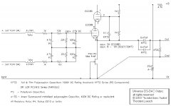
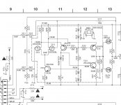
My main issue now is, that my player - unlike the easier tunable CD63/67 - has two DACs(SM5872BS) instead of one. Each of them is fed by the same integrated circuit, that modifies the I2S signal for each DAC (L/R flag and DATA content). Each DAC has four analogue outputs - normally: L+L-R+R- (two balanced channels) - here in this case one DAC has got 1L+, 2L+, 1L-, 2L-, the other has 1R+, 2R+, 1R-, 2R-. Now Marantz uses two differential buffers to get again two single balaced signals (L+L-R+R-). One more buffer (HDAM) module per side convert this signal into SE signals. So far so complicated. I hope this is understandable and right. Here the sheme:
So in my eyes I have a few options:
++ use just one of the positive outputs, i.e. 1L+ and 1R+ right off the DACs and add Thorstens tube stage.
++ use one balanced pair of each dac, add a transformer to make it SE and a tube stage
++ use the first part of the players HDAMs to summarize all the doubled channels and add a tube stage
++ build four differential tube stages followed by 2 balanced2 SE tube stage (6 double triodes)
++ deeply modify this player, deactivate one DAC, deactivate the separating IC (TC160G11AU) and feed the other DAC with an external clock and the I2S stream right out of the TDA 1302T (drive logic). As an analogue stage I'd use a tube like Thorstens one.
My questions now are:
?? Is my analysis of the circuit right?
?? Which of the options might be the best?
?? Which would be the best simple one?
Thanks for reading. Please post just positive answers! I'm not skilled, I just read a lot and have a huge amount of dangerous quarter knowledge. I might be wrong and hope to get some help here.
Cheers Ernst
I'm up to modify my CD6000OSE. I already changed most Electrolytics, some rectifiers and added some damping to the chassis.
All this made it a better player, but it is still far away from what I'd like to get - and I think that would be possible to get out of the basic concept.
I read a lot of threads here about modifying this player. Unfortunately I did not find a thread about a tubed outputstage. But this is exactly what I'd like to implement.
I know that there was a player sold under the label HEART. They added a transformer (??? for filtering AND converting balanced to SE???) and two 6922 tubes.
This player was reviewed very well. I don't know the circuit they used and I don't know how they implemented their circuit. What I found was a link to "Thermionic Valvestages" by Thorsten Loesch. He describes different DAC principles and how to implement which circuit. Well, thats it, I thought.
My main issue now is, that my player - unlike the easier tunable CD63/67 - has two DACs(SM5872BS) instead of one. Each of them is fed by the same integrated circuit, that modifies the I2S signal for each DAC (L/R flag and DATA content). Each DAC has four analogue outputs - normally: L+L-R+R- (two balanced channels) - here in this case one DAC has got 1L+, 2L+, 1L-, 2L-, the other has 1R+, 2R+, 1R-, 2R-. Now Marantz uses two differential buffers to get again two single balaced signals (L+L-R+R-). One more buffer (HDAM) module per side convert this signal into SE signals. So far so complicated. I hope this is understandable and right. Here the sheme:
So in my eyes I have a few options:
++ use just one of the positive outputs, i.e. 1L+ and 1R+ right off the DACs and add Thorstens tube stage.
++ use one balanced pair of each dac, add a transformer to make it SE and a tube stage
++ use the first part of the players HDAMs to summarize all the doubled channels and add a tube stage
++ build four differential tube stages followed by 2 balanced2 SE tube stage (6 double triodes)
++ deeply modify this player, deactivate one DAC, deactivate the separating IC (TC160G11AU) and feed the other DAC with an external clock and the I2S stream right out of the TDA 1302T (drive logic). As an analogue stage I'd use a tube like Thorstens one.
My questions now are:
?? Is my analysis of the circuit right?
?? Which of the options might be the best?
?? Which would be the best simple one?
Thanks for reading. Please post just positive answers! I'm not skilled, I just read a lot and have a huge amount of dangerous quarter knowledge. I might be wrong and hope to get some help here.
Cheers Ernst
Hmm, no reply so far... Anything wrong with my post? Questions too specific?
To be honest, I would be happy about any reply regarding tube outputs for my player. Maybe somebody knows a thread in another forum?
Thx
Ernst
To be honest, I would be happy about any reply regarding tube outputs for my player. Maybe somebody knows a thread in another forum?
Thx
Ernst
Dear community
I know that there was a player sold under the label HEART. They added a transformer (??? for filtering AND converting balanced to SE???) and two 6922 tubes.
This player was reviewed very well. I don't know the circuit they used and I don't know how they implemented their circuit. What I found was a link to "Thermionic Valvestages" by Thorsten Loesch. He describes different DAC principles and how to implement which circuit. Well, thats it, I thought.
Afaik the way Heart did it was just add a tube stage after the existing output stage. Not impressive imho.
The extra tranny was a power xformer for the tube stage.
My main issue now is, that my player - unlike the easier tunable CD63/67 - has two DACs(SM5872BS) instead of one. Each of them is fed by the same integrated circuit, that modifies the I2S signal for each DAC (L/R flag and DATA content). Each DAC has four analogue outputs - normally: L+L-R+R- (two balanced channels) - here in this case one DAC has got 1L+, 2L+, 1L-, 2L-, the other has 1R+, 2R+, 1R-, 2R-. Now Marantz uses two differential buffers to get again two single balaced signals (L+L-R+R-). One more buffer (HDAM) module per side convert this signal into SE signals. So far so complicated. I hope this is understandable and right. Here the sheme:
So in my eyes I have a few options:
++ use just one of the positive outputs, i.e. 1L+ and 1R+ right off the DACs and add Thorstens tube stage.
++ use one balanced pair of each dac, add a transformer to make it SE and a tube stage
++ use the first part of the players HDAMs to summarize all the doubled channels and add a tube stage
++ build four differential tube stages followed by 2 balanced2 SE tube stage (6 double triodes)
++ deeply modify this player, deactivate one DAC, deactivate the separating IC (TC160G11AU) and feed the other DAC with an external clock and the I2S stream right out of the TDA 1302T (drive logic). As an analogue stage I'd use a tube like Thorstens one.
My questions now are:
?? Is my analysis of the circuit right?
?? Which of the options might be the best?
?? Which would be the best simple one?
Thanks for reading. Please post just positive answers! I'm not skilled, I just read a lot and have a huge amount of dangerous quarter knowledge. I might be wrong and hope to get some help here.
Cheers Ernst
I'm curious about this also, I've been looking into adding a tube output to my Sony CDP which has dual balanced dacs as well.
I already designed a SRPP for a Philips TDA1541 with stunning results, I want more

Hello Miniwatt,Afaik the way Heart did it was just add a tube stage after the existing output stage. Not impressive imho.
The extra tranny was a power xformer for the tube stage.
I'm curious about this also, I've been looking into adding a tube output to my Sony CDP which has dual balanced dacs as well.
I already designed a SRPP for a Philips TDA1541 with stunning results, I want more
I found this on: http://www.marantzphilips.nl/review_marantz_cd6000_ose_le/
They explain:
Upgrades and Changes by Heart
Rik Stoet's Heart factory performs numerous modifications to the Marantz design. Most importantly in my opinion is that Heart disconnects the entire Marantz designed analog section (although it remains in the chassis) and substitutes a circuit using a pair of dual triode 6922 vacuum tubes. The pair is energized by two transformers, one powers the heaters, the other the anodes. The unit ends up with a total of 5 transformers, three for the power supply and 2 for the audio circuits. The printed circuit board is modified and relocated to reduce interference from the power supply.
The headphone jack has been disconnected to reduce the load on the audio section and increase performance. Additional Philips capacitors are installed in the high pass section. The transformer for 110-120 volt markets has been specially designed by Heart for use in those markets. Finally, additional damping to the chassis and transport has been added over and above that already installed by Marantz. Cosmetically, the only difference between the Marantz and the Heart unit is the addition of a small tasteful "Tubed by Heart" logo below the CD drawer.
Also I found this pic from the Heart CD6000:
There is no Opamp or HDAM visible. They route the signal out of the PCB far before the following opamp had been. And the added a clock.
I'd really like to know what they did precisely. 😕
Yes, you probably could do the same or something similar, if we found out.
By the way, which 1541 CDP have you tubed?
Cheers Ernst
Attachments

Actually, the Heart 6000 is NOT entirely tube output. The signal taken from the SM5872 dac chips is voltage out, and therefore uses each dac chip's i/v converter opamp stages before going to the coupling transformers. The Heart guys did not take this into account, and thus did not add any extra filtering or HF bypassing to the analog supply lines to the SM5872's, which can make quite a difference. Personally, I have found, among the several Heart 6000's I've worked on and upgraded, a LOT of variability in sound quality, not attributable to the tubes. I had two Heart 6000's that had identical work done(including the same version, grey-cased transformers throughout), and, even with Dutch Amperex 6DJ8's installed, one sounded dismal & the other sounded quite nice. I did a lot of work on sorting out what was causing the difference, and either there's just a bad amount of variability in the coupling transformers, or there's a really unacceptable amount of batch variability in the SM5872 dac chips.
Hi Stephen (right?),
wow, so you know the Heart 6000CDP. Thats great. Thanks for your reply 🙂
Very strange behavior. Might be the reason for some good reviews of the Marantz CD6000(OSE), even I wasn't happy at all with this CDP, when I bought it almost 10 years ago. It was a boring, dull sounding player. My expectations were much higher. So I did some mods, years ago, which resulted in better dynamics, more freshness and power. Even then I thought, this can't be the end…..
Yes I know, the SM5872 is a V-out DAC. Apparently it should be one of the better V-out types, referring to Thorsten Loesch, who wrote in his paper 'Thermionic Valvestages':
The generation before the latest designs is a bit more heterogeneous. We find many DAC’s with differential output but various different schemes of
on chip filtering and buffering and the occasional DAC with a single-ended output and really good on chip analogue silicon. In the latter case
(CS4328, certain OEM Products) the same as above holds true. For all other differential output DAC’s the circuit shown further down should/could
be used and should work under any conditions, offering good filtering and ensuring an easy load for the DAC Chip, keeping distortion low.
Finally, the original first-generation timeslicing DAC’s have no analogue stages. Some of these are early Philips chip’s as used in the QED "Digit"
external DAC, also the NPC SM5872 (Marantz CD-53/57/63/67 among others) and NPC SM5864 (Arcam Alpha - lower Models) and surprisingly
many OEM chips even in current use. All these will require some buffering and due to the lack of on chip filtering a direct connection without any
additional lowpass filtering a direct connection even to high impedance inputs is not advisable. Again, the circuit shown below will work just fine.
That’s why I started thinking about adding tubes to this player. Thorstens circuit includes filtering and puts load to the balanced signal too, although this signal is not used by the following stage. Almost perfect, if there wouldn't be the second channel per DAC.
You'd probably know, which outputs (of the 4 per DAC (2 pos and 2 neg )) the Heart guys used to feed the transformer with. It would be great if I could get this info. This would help me deciding how to move on.
Thanks a lot
Ernst
Attachments
I never got a schematic for the 6000 series, nor do I currently have one of the players on hand, but, as I recall, the 5872's were connected much like Pioneer does with their PD65/75 level 'pulseflow' stereo dacs, where they sum R+ & L+ via some small value resistors, and do likewise with the negative outs. This would certainly make sense with the 5872, given what Loesch says about output current(implies, at least) on these. BTW, the datasheet for the SM5872(which I googled easily) DOES show analog buffer(at least) stages before the chip's outputs, and I definitely can attest to the benefit of being very generous with the size & quality of supply caps next to the analog supply line pins.
As you may guess, I believe one must first find a 6000 that actually sounds OK to start with, as the dismal sounding ones tend to retain some of that no matter what upgrades one does to them.
As you may guess, I believe one must first find a 6000 that actually sounds OK to start with, as the dismal sounding ones tend to retain some of that no matter what upgrades one does to them.
Hi guys, I don't know much about valve output for the cd6000, but in my experience, adding a really good, low-noise reg to power the dacs and separator chip is the only way I managed to remove the ragged treble sound, and this was after clocking too. There's a 7805 reg on the board that does the job already, but with a really good reg in there, the difference is amazing. I've done this mod two or three times now to different cd6000's.
Cheers, Lee.
Cheers, Lee.
SM5872 requires external subtractio of the DAC+ and DAC- outputs:
DACOUT=(DAC+)-(DAC-).
If differential out is to be preserved, you must do this twice:
DACOUT+=(DAC+)-(DAC-)
DACOUT-=(DAC-)-(DAC+)
The reason this operation must be done to gt the full DAC performance is twofold:
Firstly, the DAC outputs are 'quasi-differential' - this is the term used in the data sheet. The outputs are pulses 0 to 12 MCLK cycles in length occuring every 12 MCLK cycles (0% to 100% duty cycle, at 32FS). Odd lengths of pulses (1, 3, 5, etc) cannot be symetrically centered around the middle of each 12-pulse PWM modulation cycle, so if something is not done about that, each odd length PWM pulse is 1 MCLK cycle out of phase - i.e. a 1 MCLK cycle jitter correlated with the output level is generated. To prevent this, the DAC+ and DAC- outputs are out of phase by 1 cycle for odd length combinations, and recreating a single ended pulse from these results in a 'halftoned' pulse which is centered around the midde of each 12 MCLK PWM modulation cycle, preventing the introduction of jitter. Becasue this jitter is introduced at the low resolution end of the sigma-delta DAC, the noise and distortion generated when only one of the differential outputs is used, without subtraction, is very high (and very audible).
Secondly, becuase the rate of PWM pulses is quite low (32Fs, whereas 64, 96, 128 or 192 Fs or even higher is more common), it appears that quite deep dithering/noise shaping is used to get adequate performance. Based on measuring peak values of the signal at the DAC+ and DAC- outputs, vs RMS post filtering, it appears that as many as 4 levels out of the 13 possible PWM output levels can contain residual quantizing noise.
Even though this is pushed higher in the spectrum by noise shaping, the low rate of PWM pulses means the rise of the noise floor is noticeable while still inside the audio band, rising as you go to the high end of it. In order to considerably reduce this problem, the noise shaping is actually common mode across DAC+ and DAC- outputs, and some care was obviously taken to prevent colision of this scheme with the quasi-differential out-of phase PWM trick described above. When only one DAC output is used without subtraction, the noise is clearly audible for a digital zero at the DAC input (this largely prevents jitter artifacts described in the previous paragraph from appearing as added noise). When proper subtraction is used, the DAC stays dead silent within the audio band.
In other words, if you only use one output, you get a large loss in resolution, a large increase in residual noise and an even larger introduction of jitter - 1 MCLK correlated jitter in most implementations means 59ns peak to peak jitter, compare this with picosecond speciffications on MCLK source clocks needed to get the most out of the DAC. So, with all respect to Thorsten, the above schematic is NOT recommended for this particular DAC, even though it is electrically correct.
If you ever needed, I could support you with the manual, showing the scheme.I never got a schematic for the 6000 series, nor do I currently have one of the players on hand
Interesting Idea - I'll look after the manual.but, as I recall, the 5872's were connected much like Pioneer does with their PD65/75 level 'pulseflow' stereo dacs, where they sum R+ & L+ via some small value resistors, and do likewise with the negative outs.
Really strange but might be that way. After my early mods, good rectifiers - very good electrolytics - removed output elkos - removed mute transistors, slight damping of the chassis most people (the normal ones, not addicted onesBTW, the datasheet for the SM5872(which I googled easily) DOES show analog buffer(at least) stages before the chip's outputs, and I definitely can attest to the benefit of being very generous with the size & quality of supply caps next to the analog supply line pins.
As you may guess, I believe one must first find a 6000 that actually sounds OK to start with, as the dismal sounding ones tend to retain some of that no matter what upgrades one does to them.
) would be happy with it. Unfortunately I've heard a few really good sounding CDPs. 🙄I thought about doing that, but never did so far. Good advice, thanks - will do since it is a rather easy mod.Hi guys, I don't know much about valve output for the cd6000, but in my experience, adding a really good, low-noise reg to power the dacs and separator chip is the only way I managed to remove the ragged treble sound, and this was after clocking too. There's a 7805 reg on the board that does the job already, but with a really good reg in there, the difference is amazing. I've done this mod two or three times now to different cd6000's.
🙂😕😱SM5872 requires external subtractio of the DAC+ and DAC- outputs:
DACOUT=(DAC+)-(DAC-).
If differential out is to be preserved, you must do this twice:
DACOUT+=(DAC+)-(DAC-)
DACOUT-=(DAC-)-(DAC+)
The reason this operation must be done to gt the full DAC performance is twofold:
Firstly, the DAC outputs are 'quasi-differential' - this is the term used in the data sheet. The outputs are pulses 0 to 12 MCLK cycles in length occuring every 12 MCLK cycles (0% to 100% duty cycle, at 32FS). Odd lengths of pulses (1, 3, 5, etc) cannot be symetrically centered around the middle of each 12-pulse PWM modulation cycle, so if something is not done about that, each odd length PWM pulse is 1 MCLK cycle out of phase - i.e. a 1 MCLK cycle jitter correlated with the output level is generated. To prevent this, the DAC+ and DAC- outputs are out of phase by 1 cycle for odd length combinations, and recreating a single ended pulse from these results in a 'halftoned' pulse which is centered around the midde of each 12 MCLK PWM modulation cycle, preventing the introduction of jitter. Becasue this jitter is introduced at the low resolution end of the sigma-delta DAC, the noise and distortion generated when only one of the differential outputs is used, without subtraction, is very high (and very audible).
Secondly, becuase the rate of PWM pulses is quite low (32Fs, whereas 64, 96, 128 or 192 Fs or even higher is more common), it appears that quite deep dithering/noise shaping is used to get adequate performance. Based on measuring peak values of the signal at the DAC+ and DAC- outputs, vs RMS post filtering, it appears that as many as 4 levels out of the 13 possible PWM output levels can contain residual quantizing noise.
Even though this is pushed higher in the spectrum by noise shaping, the low rate of PWM pulses means the rise of the noise floor is noticeable while still inside the audio band, rising as you go to the high end of it. In order to considerably reduce this problem, the noise shaping is actually common mode across DAC+ and DAC- outputs, and some care was obviously taken to prevent colision of this scheme with the quasi-differential out-of phase PWM trick described above. When only one DAC output is used without subtraction, the noise is clearly audible for a digital zero at the DAC input (this largely prevents jitter artifacts described in the previous paragraph from appearing as added noise). When proper subtraction is used, the DAC stays dead silent within the audio band.
In other words, if you only use one output, you get a large loss in resolution, a large increase in residual noise and an even larger introduction of jitter - 1 MCLK correlated jitter in most implementations means 59ns peak to peak jitter, compare this with picosecond speciffications on MCLK source clocks needed to get the most out of the DAC. So, with all respect to Thorsten, the above schematic is NOT recommended for this particular DAC, even though it is electrically correct.
So does this mean that best I leave the outputsage, as it is or, if I wanted a tubed one, I have to build right in the way the current silicium one is?
Thanks a lot. Even I have to think about that hard, I already have learned a lot.
Cheer Ernst
By the way, which 1541 CDP have you tubed?
Cheers Ernst
Hi Ernst,
A Philips CD650.
The NPC Sm5872 indeed has no analog output stage in the traditional sense, and in fact, this may be considered a plus, because you can build your own in any way you please.
I have quite extensive experience with this chip along with a few others that are similar (from Sony, Pioneer, Philips). All these DACs have raw push-pull square wave outputs using various schemes of modulation, the NPC in particular uses a PWM scheme to implement a multilevel DAC output, with 13 levels (0 to 12 out of 12 pulse width 'slots' high, the rest low). This can easily be verified with a scope. Only the two outputs together contain the proper output information, see what I wrote about the quasi-differential scheme it uses in my post above - see figure 12 on page 21 of the SM5872 datasheet.
There are a couple of things to take care of in order to get best performance out of this DAC, before you even get to the analog output stages.
Firstly, the actual voltages that the LO/LON and RO/RON outputs present are determined by the pins AVss1,2,3,4 and AVdd1,2. In particular, AVss determines the low output voltage, and should be treated as the analog ground of the DAC (not to be confused by the separate analog ground pin for the built-in oscillator!). AVdd pins determine the high output voltage, and should be considered the DAC analog power supply. The output stage simply switches AVdd to the corresponding output for a high state, and AVss for a low state, using MOSFETs - see the block diagram on page 2 of the datasheet. The specs for AVss and AVdd dictate that AVss should be as close to 0 as possible, and AVdd should not be more than +-05V different than DVdd - if you plan on giving them a separate clean power supply (a VERY good idea!), protection diodes should be used between AVdd and DVdd to prevent chip latch-up at power on and power off.
This scheme of operation means that the DAC effectively multiplies AVss with the digital value given to it, to create the output voltage - so any changes in AVss DIRECTLY modulate the output of the DAC!!!. Proper filtering and regulation is required here - when I wrote 'any changes', this means any ripple, noise, clock cross-coupling, power line sag, digital hash injected from other parts of the player, etc. These lines need to be super clean. Yet, in most players they are not even decoupled from the rest of the power supply - for instance, in the Marantz CD63, even though a simple RC filter is included in the layout of the PCB, these are DIRECTLY connected to the DIGITAL power supply by jumpers!!! - even in the KI version. Do not avoid proper decoupling caps here - current passed through these pins contains signifficant amounts of spectral energy at the MCLK frequency, which will typically be 384Fs.
Secondly, the datasheet hides the spec for output impedance like a snake would hide legs. It only gives two very similar examples for output stages. In theory, the less they are loaded, the better the output waveform. The problem with very high load impedances is that very low value capacitors should be used in filters so stray capacitances and input capacitances of other components become a large contributor. Considering that some of these may be highly non-linear (OP-AMP inputs...), this approach should be used with caution. It is valid, though, for tube output stages, where input capacitances are vacuum, but keep in mind that miller capacitances are only as linear as the tube itself. A better approach would be to use lower impedances.
Because of the quasi-differential scheme used by this DAC, it is highly advisable to use a passive output filter at least in the first and preferably in all stages. This way filtering out high frequency components is handled by much more easily controlled passive components. Experiemnts have shown that the SM5872 can drive output impedances on the order of a few k ohms with no degradation of output waveform, which gives filter cap values in the order of hundreds of pF. This should be sufficient to swamp out strays and other similar contributions to the actual capacitors in the filter circuit.
My personal favorite arrangement would be to use a differential capacitor for the first stage of filtering (see figure 19 page 25 of datasheet, the part before the op-amps), which will keep most residual HF hash resulting from the quasi-differential PWM output scheme confined in a small current loop close to the actual DAC chip. The other stages can be standard with a common ground, like on Thorstens schematic. However, the two outputs should be subtracted at the end using a differential amplifier - you can't avoid this even with a tube output stage. There is another way it can be done that entails signal manipulation at the PWM output itself, but this requires a lot of knowledge in high frequency digital PCB design. In any case, some form of diff-to-singleended conversion is mandatory, and so is buffering.
Thirdly, and possibly redundant of me to mention, is that the clock shuld have as low a jitter as possible. Because the actual PWM modulation frequency is not as high as in some other converters of this type, jitter sensitivity is also lower but still, like all low-bit SD type DACs, thsi one is very sensitive to jitter. Surprisingly, quite good performance is achievable even eith the built-in clock oscillator, IF proper care is taken to give it a good, clean and low noise power supply, and of course, a proper local ground connetction. The limitations are similar to AVdd, XVdd should not appear before DVdd, or persist after DVdd - easily satisfied with a few diodes.
Finally, the real limiting factor of this chip is the built-in digital filter, which is a simplified version of the stand-alone DFs NPC used to build at the same time - in either case, compared to today's standards it's definitely far from the pinancle of performance, so in essence this DAC is truly built for Red Boojk applications - providing 16 bits of output resolution.
Last edited:
Hi, good evening
After reading all above, I understand why most professional tuners like AH never worked with CD6000 🙄
@Miniwatt
Some consider the 960 a really really good CDP with some mods. Have you done the stage referring to Lukasz?
Seems that infos from ILIMZN are perfect for you as well 🙂
Beside my ol' CD6000 I'm working on a Grundig 8400MKII (TDA1541 too) and a CD5000 (TDA1549). Second one is really simple to modify up to a certain level. Just better caps, diodes, more ad better voltage regulation, some damping of the flimsy box and tube out stage. Nice sound. And I'm curious about the Grundig.
@ ILIMZN
Again thanks for this really deep view into the modus operandi of this DAC. Never expected that!
Took me a while to think that I understood most of that. Might be that still I'm not clear with all that. Your highlighted line said: This scheme of operation means that the DAC effectively multiplies AVss with the digital value given to it, to create the output voltage - so any changes in AVss DIRECTLY modulate the output of the DAC!!!. Why do they multiply the ground?
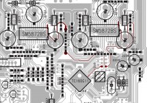
You wrote further: Clean Voltage is mandatory for really good output and built in clock can be rather good with clean juice. Looking at the traces on the PCB leading clocksignal from separation chip (TC160G11AU – btw never found a Specsheet of this IC) to DACs is awfully long and wounded as you can see on the added jpg. Would it help to replace these meanders? Or did you mean SM5872 built in clock generally?
So you gave me a lot of information to get best out of this DAC. Some more questions I consider still important:
+++ Since I have 2 DACs, one for left and one for right side, I assume both output-channels on one DAC put out exactly the same signal. OK? (my assumption: TC160G11 separates signal and sends doubled singleside - signal to each DAC)
+++ Is there an advantage using summarized signal vs. using just one + - pair per DAC?
+++ If there is an advantage using summarized signal (stronger signal (higher current) , higher precision, …) , is it possible to summarize them as stevensank mentioned in his post, referring to Pionier PD55, just by using some KOhms of resistance? Second pic is about that.
@ stevensank
considering all recent infos , the difference in sound of various CD6000 might come from sample variation of the 7805 regulators? Just an idea, don't know if there is significant variation. Have you modified the PSU in these players as well?
Ernst
After reading all above, I understand why most professional tuners like AH never worked with CD6000 🙄
@Miniwatt
Some consider the 960 a really really good CDP with some mods. Have you done the stage referring to Lukasz?
Seems that infos from ILIMZN are perfect for you as well 🙂
Beside my ol' CD6000 I'm working on a Grundig 8400MKII (TDA1541 too) and a CD5000 (TDA1549). Second one is really simple to modify up to a certain level. Just better caps, diodes, more ad better voltage regulation, some damping of the flimsy box and tube out stage. Nice sound. And I'm curious about the Grundig.
@ ILIMZN
Again thanks for this really deep view into the modus operandi of this DAC. Never expected that!
Took me a while to think that I understood most of that. Might be that still I'm not clear with all that. Your highlighted line said: This scheme of operation means that the DAC effectively multiplies AVss with the digital value given to it, to create the output voltage - so any changes in AVss DIRECTLY modulate the output of the DAC!!!. Why do they multiply the ground?
You wrote further: Clean Voltage is mandatory for really good output and built in clock can be rather good with clean juice. Looking at the traces on the PCB leading clocksignal from separation chip (TC160G11AU – btw never found a Specsheet of this IC) to DACs is awfully long and wounded as you can see on the added jpg. Would it help to replace these meanders? Or did you mean SM5872 built in clock generally?
So you gave me a lot of information to get best out of this DAC. Some more questions I consider still important:
+++ Since I have 2 DACs, one for left and one for right side, I assume both output-channels on one DAC put out exactly the same signal. OK? (my assumption: TC160G11 separates signal and sends doubled singleside - signal to each DAC)
+++ Is there an advantage using summarized signal vs. using just one + - pair per DAC?
+++ If there is an advantage using summarized signal (stronger signal (higher current) , higher precision, …) , is it possible to summarize them as stevensank mentioned in his post, referring to Pionier PD55, just by using some KOhms of resistance? Second pic is about that.
@ stevensank
considering all recent infos , the difference in sound of various CD6000 might come from sample variation of the 7805 regulators? Just an idea, don't know if there is significant variation. Have you modified the PSU in these players as well?
Ernst
Attachments
Hi, good evening
...
@ ILIMZN
Again thanks for this really deep view into the modus operandi of this DAC. Never expected that!
Took me a while to think that I understood most of that. Might be that still I'm not clear with all that. Your highlighted line said: This scheme of operation means that the DAC effectively multiplies AVss with the digital value given to it, to create the output voltage - so any changes in AVss DIRECTLY modulate the output of the DAC!!!. Why do they multiply the ground?
Sorry, typo - I meant AVdd-Avss (supply voltage between AVdd and AVss). In practise since AVss is the analog ground and nominally 0 V, and AVdd is referenced to it, you could say it multiplies AVdd with the digital input - this of course refers to the result of LO-LON or RO-RON, i.e. differential voltage between these pins. In practise, however, it is more like K*AVdd*[binary in], where K is less than 1, actually approximately 0.62. The DAC cannot achieve full modulation of it's PWM outputs due to some headroom used for the residual noise from noise shaping and dithering. So, When AVdd is 5V, the output is 2.2V RMS nominal, instead of the theoretical 3.54V using AVdd as the maximum peak value.
You wrote further: Clean Voltage is mandatory for really good output and built in clock can be rather good with clean juice. Looking at the traces on the PCB leading clocksignal from separation chip (TC160G11AU – btw never found a Specsheet of this IC) to DACs is awfully long and wounded as you can see on the added jpg. Would it help to replace these meanders? Or did you mean SM5872 built in clock generally?
I meant SM5872 built in clock oscillator. This is not used in your player. The TC160G11AU is a mask programmable gate array chip made by Toshiba. It's function is determined by the last metalisation mask in the manufacturing process - you can think of it as a one-time programmable FPGA. The data separation logic is implemented in it.
It also distributes the clock - the oscillator is elsewhere (can't see it in the jpeg...). According to SM5872 specs, external clock is fed into the XTAL input pin, if I remember correctly. The clock that then ends up distributed to the internals of the SM5872 should be visible on the XTAL out pin - a good pointer of it's quality should be the shape of the clock pulses as observed with a good scope and probe. It is still highly recomended that the XVss and XVdd pins be fed with a clean supply because the clock signal still passes through the SM5872 clock buffer circuitry - the power for this is supplied by XVdd, ground by XVss. Any garbage present here will of course result in added jitter to the internal SM5872 clock.
So you gave me a lot of information to get best out of this DAC. Some more questions I consider still important:
+++ Since I have 2 DACs, one for left and one for right side, I assume both output-channels on one DAC put out exactly the same signal. OK? (my assumption: TC160G11 separates signal and sends doubled singleside - signal to each DAC)
THis is something I cannot be sure about without the schematic of the analog output stage. You can use two schemes - one uses exactly the same signal for both channels, the other uses one channel as an inverted version of the other. It is also possible for the TC160G11 to include other forms of manipulation of the signal, like a form of dynamic element matching, to improve the resolution of the dac or lower residual noise. You could only determine this by measurement.
I should point out one important thing here. If you input data single channel data as L and the same inverted data as R, the DAC will NOT output an inverted version of LO/LON on the RO/RON pins! This means that although the DAC is operated in differential fashion in this way, and RON is essentially the same as LO with a small DC offset (ditto for RO and LON), you cannot just sum LO and RON or LON and RO and get proper output. Sigma-Delta DACs are notorious for generating different sequences for different DC offsets and inversion introduces an offset of -1 LSB. Because of this the quasi-differential PWM scheme does not cancel out between LO and RON or LON and RO, so the 1 MCLK jitter introduction still applies. Unfortunately, the need for subtraction still applies.
That being said, what you would actually be doing is (LO-LON)-(RO-RON). Because RO/RON carry the inverted LO/LON, and RON is conceptually RO inverted (same is true for the LON/LO pair), you could say (disregarding the small DC offset for the moment) that LO==RON and RO==LON. So, the actual operation based on the formula above is LO-LON-RO+RON, which is really (LO+RON)-(RO+LON). Not obvious, but this means that you can add (LO+RON) and (RO+LON) using simple resitors, and then use their value in parallel as the first resistor in a single differential filter. What this means is, the impedances in the filter appear smaller, so caps can be larger, and more current can be supplied from the DAC - twice as much. Lower impedances also reduce noise generated by OP-amp input noise current - by 6dB. Careful derivation of all the maths will also show that the quasi-differential PWM scheme still successfully cancels out even though only one differential amp is needed at the output. Also, because the digital input codes have one more code available for negative values (+32767, -32768), this scheme cancels out the (admittedly very small) offset inherent to this type of coding. Finally, the noise generated by the DAC is reduced. However, it is impossible to say exactly how much further the residual noise from noise shaping and dithering is reduced - this reduction relies on different sequences being generated for the true and inverted versions of the input signal, which also mean the noise shaping noise is different, but not vompletely non-correlated (completely non-correlated npise would be reduced by 3dB, in this case the reduction is less and may even increase in some cases). The dithering noise, however, is usually the same but antiphase and this scheme will completely cancel it out - again, wether this is a good thing, depends on the actual implementation of the internals of the DAC. Here, I am afraid, I have no further knowledge of how the SM5872 works.
Finally, if the same signal is fed to both channels of the DAC, reduction in noise due to lower series impedances in the filter still applies (you can still add same phase signals via resistors as part of the first stage of filtering), as well as the analog noise contribution of the DAC output circuits (but this should be negligible). The noise shaping and dithering are the same so no canceling out or decorrelating is present - this portion stays the same.
It should be noted that using a large number of such DACs in parallel may decrease the output impedance enough to be able to drive a high impedance input directly from the passive filter network, BUT this would have to be a true differential input with common mode canceling - you guessed it, because of the quasi-differential PWM scheme.
+++ Is there an advantage using summarized signal vs. using just one + - pair per DAC?
+++ If there is an advantage using summarized signal (stronger signal (higher current) , higher precision, …) , is it possible to summarize them as stevensank mentioned in his post, referring to Pionier PD55, just by using some KOhms of resistance? Second pic is about that.
I believe I answered that above. It should be noted that it is possible, in theory, to increase the resolution by 1 bit depending on the type of manipulation done by the gate array. However, i doubt this is the case as the input to the SM5872 is limited to 16 bits by design, and this is what the built-in digital filter expects - as I said, this is the real bottleneck in this DAC.
Hi Enzdone,
thanks, I've read almost everything from Lukasz. He personally didn't a SM5278, but some friends. They just used R(L)O, single ended without subtraction of the quasi differential R(L)ON signal. Lukasz told me to do it the same way, that this is ok, since the R(L)ON signal is ceated artificially anyway. I wasn't sure about that after digging into the circuit a bit and thats why I asked here. I like to read his pages, his approach is always interesting and entertaining.
I meant SM5872 built in clock oscillator. This is not used in your player. The TC160G11AU is a mask programmable gate array chip made by Toshiba. It's function is determined by the last metalisation mask in the manufacturing process - you can think of it as a one-time programmable FPGA. The data separation logic is implemented in it.
It also distributes the clock - the oscillator is elsewhere (can't see it in the jpeg...). According to SM5872 specs, external clock is fed into the XTAL input pin, if I remember correctly. The clock that then ends up distributed to the internals of the SM5872 should be visible on the XTAL out pin - a good pointer of it's quality should be the shape of the clock pulses as observed with a good scope and probe. It is still highly recomended that the XVss and XVdd pins be fed with a clean supply because the clock signal still passes through the SM5872 clock buffer circuitry - the power for this is supplied by XVdd, ground by XVss. Any garbage present here will of course result in added jitter to the internal SM5872 clock.
Ilimzn, I think, the oscillator is close to the TC160G11, on the right side of the IC. There is a quarz, 16.xxx MHz, part 5310, there are 2 Caps pasts 2329 and 2330. The brown traces in my jpg (in last) post then lead to the DACs and end in XTI. Teh XTO is floating. So they are supported as there were an external clock. Just for info. Probably best would be adding an external clock that goes directly to separator chip and to both of the DACs.
THis is something I cannot be sure about without the schematic of the analog output stage. You can use two schemes - one uses exactly the same signal for both channels, the other uses one channel as an inverted version of the other. It is also possible for the TC160G11 to include other forms of manipulation of the signal, like a form of dynamic element matching, to improve the resolution of the dac or lower residual noise. You could only determine this by measurement.
I should point out one important thing here. If you input data single channel data as L and the same inverted data as R, the DAC will NOT output an inverted version of LO/LON on the RO/RON pins! This means that although the DAC is operated in differential fashion in this way, and RON is essentially the same as LO with a small DC offset (ditto for RO and LON), you cannot just sum LO and RON or LON and RO and get proper output. Sigma-Delta DACs are notorious for generating different sequences for different DC offsets and inversion introduces an offset of -1 LSB. Because of this the quasi-differential PWM scheme does not cancel out between LO and RON or LON and RO, so the 1 MCLK jitter introduction still applies. Unfortunately, the need for subtraction still applies.
That being said, what you would actually be doing is (LO-LON)-(RO-RON). Because RO/RON carry the inverted LO/LON, and RON is conceptually RO inverted (same is true for the LON/LO pair), you could say (disregarding the small DC offset for the moment) that LO==RON and RO==LON. So, the actual operation based on the formula above is LO-LON-RO+RON, which is really (LO+RON)-(RO+LON). Not obvious, but this means that you can add (LO+RON) and (RO+LON) using simple resitors, and then use their value in parallel as the first resistor in a single differential filter. What this means is, the impedances in the filter appear smaller, so caps can be larger, and more current can be supplied from the DAC - twice as much. Lower impedances also reduce noise generated by OP-amp input noise current - by 6dB. Careful derivation of all the maths will also show that the quasi-differential PWM scheme still successfully cancels out even though only one differential amp is needed at the output. Also, because the digital input codes have one more code available for negative values (+32767, -32768), this scheme cancels out the (admittedly very small) offset inherent to this type of coding. Finally, the noise generated by the DAC is reduced. However, it is impossible to say exactly how much further the residual noise from noise shaping and dithering is reduced - this reduction relies on different sequences being generated for the true and inverted versions of the input signal, which also mean the noise shaping noise is different, but not vompletely non-correlated (completely non-correlated npise would be reduced by 3dB, in this case the reduction is less and may even increase in some cases). The dithering noise, however, is usually the same but antiphase and this scheme will completely cancel it out - again, wether this is a good thing, depends on the actual implementation of the internals of the DAC. Here, I am afraid, I have no further knowledge of how the SM5872 works.
Finally, if the same signal is fed to both channels of the DAC, reduction in noise due to lower series impedances in the filter still applies (you can still add same phase signals via resistors as part of the first stage of filtering), as well as the analog noise contribution of the DAC output circuits (but this should be negligible). The noise shaping and dithering are the same so no canceling out or decorrelating is present - this portion stays the same.
It should be noted that using a large number of such DACs in parallel may decrease the output impedance enough to be able to drive a high impedance input directly from the passive filter network, BUT this would have to be a true differential input with common mode canceling - you guessed it, because of the quasi-differential PWM scheme.
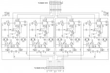
again WOW. Have to go throught this slowly!!! Do some measurements and hope that my 50MHZ skope is good enough to show what I need to see. BTW, here are two pics of the two stages. First shows the first stage for both channels (at least in the CD6000 - the CD6000OSE has got for HDAM ircuits instead - pic 3) and from the second stage only one channel.You say, with some limitation this DAC has very useful functions and characteristis. For me it seems to be a very complicated item.
Old TDA DACs seem to be more simple to work with. So I ask a delicate and naive question, if this DAC is better and/or cheaper in production than the old TDAs? Please no big discussion, I just want to know if the effort with this item, since it seems so complicated vs. the old ones, pays in terms of production (for the company, not myself) and sonically wise. In any case I'll try to get out the best I can in different steps.
First will be to optimize the powersupply up to a certain level.
Second will be an optimized clock
Later I'll start working on the outputstage. Will take some time! Winter is coming, time to make experiments.
After having finished I'll post again, or in case of, I'll ask further questions. The devil is in the details 😱
Cheers Ernst
Attachments
Last edited:
They just used R(L)O, single ended without subtraction of the quasi differential R(L)ON signal. Lukasz told me to do it the same way, that this is ok, since the R(L)ON signal is ceated artificially anyway.
Most of the experience with the SM5872 i gathered on a marantz CD1020, which is really a CD43/53/63 in disguise (without the HDAM modules). This I have 'modded to death' and in the course of it, things first started to get more and more complicated with more and more regulators, until I really started to look at the datasheets and then thinghs got to be simpler and simpler, for the same or even better results. Let me explain some of my findings and decisions:
The CD1020 has a fancy output muting and switching scheme which is the first thing I pulled out. It also uses the same output filter arrangement (OP-amp in front of the HDAM) as a CD63, which, like most such constructions (including the one in the CD6000!) is inherently flawed because it presents a different impedance to the LO and LON (and RO/RON respectively) outputs, resulting in errors of the filtering characteristics - particulairly at HF, where the impedance on one of the inputs is dictated by how well the OP-amp is capable of working at the SM5872 fundamental PWM frequency, which is 32Fs - 1.4112MHz. Very few OP-amps are well behaved at this frequency, the classic NE and NJM uparts used in these players are NOT one of them.
Things get much better if most of the filtering is done passively, then summed by a real so-called measurement differential amp topology. This requires 3 amps per channel (or 4 if you want differential outputs as well) - the circuit used in the CD63 saves one OP-amp. What puzzles me in the CD6000 schematic is that they just copy-pasted the same thing for both of the signals comprising a differential output, when they could have used the 'propper' arrangement with the same number of parts, and maybe even less parts.
In the CD1020/CD63 there is space for only one double OP-amp per channel so initially i did the same thing as described above - used just the LO and RO outputs. It sounded about right but was surprisingly noisy - so much so you could see the residual on the output with a scope - a lot of HF hash, even when the player was not playing (the DAC gets a digital zero while the player is in stop mode). The idea that these were remains of the noise-shaping and quasi-diff PWM output coding came when i noticed the hash looked exactly the same on both channels. When I switched one channel to the xON output, and summed the outputs using two equal resistors, the hash cancelled itself out! Of course, moving back to the proper 3-OPamp differential arrangement and passive filtering resulted in a noise-free output, because this arrangement subtracts the xON signal from the xO signal. It also alowed me to use a different type of OP-amp for the post-filter part and output part.
The next revelation came by listening to a full scale very low frequency sine (I burn a test CD with such signals for measurement purposes) on high impedance headphones through a small coupling cap. This alowes me to get some sort of signal through the DAC but filter out only the HF components and listen to them on headphones. What you hear is normally the feedthrough of various electrical noises generated by other parts of the player. This was a surprise - there was a lot of it. Looking at the output with a scope, I could see some quasi-periodic hash modulated in amplitude by the LF sine wave. Listening to it revealed the standard clicks and squeals of the servo and digial electronics disturbing the power supply voltage. Putting the headphones via the same coupling cap to the power supply lines revealed exactly the same sounds just louder. Checking the schematics and actual PCB revealed that AVdd was connected un-filtered to the digital power supply, with some hunderd mV of hash superimposed onto it - horrible!
A proper regulator cured this, and completely cleaned up the output of the DAC. Prompted by this finding I looked at the XTAL oscilator - the CD1020/CD63 uses the one built into the SM5872. The situation was better but not by a lot, so in went another shunt regulator.
All in all I did a LOT of mods around the DAC and clock and output. I did not try tubes simply because I currently use an approach that lets me completely avoid all amplification after the DAC itself and use a low impedance passive filter with nothing else. This, however, requires some very fast logic chips and a two-layer PCB board with extensive decoupling and voltage regulation to implement properly, and also incidentally, generates a differential output from a single SM5872. It also requires a top-quality clock generator. We can discuss this at some later time via private messages.
Ilimzn, I think, the oscillator is close to the TC160G11, on the right side of the IC. There is a quarz, 16.xxx MHz, part 5310, there are 2 Caps pasts 2329 and 2330. The brown traces in my jpg (in last) post then lead to the DACs and end in XTI. Teh XTO is floating. So they are supported as there were an external clock. Just for info. Probably best would be adding an external clock that goes directly to separator chip and to both of the DACs.
Before you do that, check that the clock on the XTAL pins and the clock outputs to the SM5872 are not inverted. I don't think the gate array uses the full 384Fs clock directly in any way, but it is worth checking just in case. If it turns out you need an inverter for one of these clocks (to the gate array OR SM5872), feed the clock directly to the SM5872, and use one of it's XTO outputs to feed the gate array, or an external inverter to feed the gate array. in any case, make sure the clock to the DAC is the most direct one with no active components inbetween to prevent adding any jitter.
use a good 100MHz probe and it should be perfectly enough. If you observe excessive ringing on the colck waveform, you might want to increase the series resistor from the gate array to the DACs (or see what i wrote about an external clock).
BTW, here are two pics of the two stages. First shows the first stage for both channels (at least in the CD6000 - the CD6000OSE has got for HDAM ircuits instead - pic 3) and from the second stage only one channel.
From what I can see, the CD6000(SE) drive the DACs in differential mode, meaning the left output is an inverted version of the right output. The gate array therefore gives each DAC the true data on one channel and the same data but inverted on the other. It is again surprising they did not do resistive summation in the filter itself, like I mentioned in my previous post, they could have saved themselves a fair number of passive components, lowered the nosie and use the existing OP-amps and HDAM to create a completely differential architecture. The good news is, you could do this yourself externally, probably even on the same board with some coponent relocations etc. I will try to find my solution for this for the CD63, whichis actually applicable nearly as-is, with the difference that the third op-amp per channel is in your case the HDAM module - but t hey are using it as such anyway.
You say, with some limitation this DAC has very useful functions and characteristis. For me it seems to be a very complicated item.
Old TDA DACs seem to be more simple to work with. So I ask a delicate and naive question, if this DAC is better and/or cheaper in production than the old TDAs? Please no big discussion, I just want to know if the effort with this item, since it seems so complicated vs. the old ones, pays in terms of production (for the company, not myself) and sonically wise.
You have to keep in m ind that it is a pulse DAC, which makes it very different from the standard multilevel TDA type DACs, either current or voltage output. because of this it's not so much more complicated to use, but different. Also, the datasheet is written ina rather convoluted way so you really have to already know how these chips work internally to understand what the datasheet is saying in some places, or sometimes, see things from the specs and diagrams, that are not explicitly mentioned in the datasheet.
Also, keep in mind that this chip also integrates several parts which are normally found separated in the older generations of CD players, such s the clock generator, the digital filter and the actual DAC - so, more to think about in order to get t he full benefit of the design.
However, unlike multilevel chips, this chip is actually not analog in the true sense of the word. because of this, it is cheaper to produce and, also, implement - but this is what generally happens as technology progresses. Keep in mind that manufacturers often create product lines by deliberatrely cuting down on the implementation of one top-level platform, which means that in essence they are deliberately 'worsening' a reference design, by omitting parts and not exactly following recomendations of the chip manufacturer. The key to restoring full capability is understanding where they did that, and in this case you are looking at different approaches compared to the previous generation TDA chips. As to how the final maximum specs compare, it is difficult to judge this objectively - and evenif one tried to keep it that way, the ear is ultimately the final judge. Great sounding devices have been produced using all the past and current DAC technologies.
Last edited:
Good Evening Ilimzn,
slowly there is light coming into this dark matter 🙄
It seems, that this player is getting a few modifications - but different from that I thought, before I started this thread.
including the output electrolytics.
Result: Clock on sep. chip has a lamda 60ns (=> 16.9 MHz), a very nice sine curve. Separation chip sends a slightly deformed, inverted curve of same frequency to the DACs. As you assumed, I'd need a phaseshifter in case of modifying not just the clock as it is routed now.
Since you went further after all your moddings and choose a very different approach - just passive filtering - I assume, the sound got even better than. Very interesting!! Of course, but later. Is your CD1020 still your main player? Is it sounding so good? Or has it got the status of an object of science only?
Well, at first I'll start, as I noted earlier, looking for better and separated voltage regulation for the dac (so far I've not decided which curcuit I should choose (TL431, Zener, discrete serial, commercial shunt regulator $$$ 😱 - any proposal?). There are lot of different loads sucking on the 5V regulator. Later I'll implement a better clock, which I alrady have.
Later I'd like to modify the outputstage. Even I asked for tubes right at the beginning, tubes are not mandatory. I just thought, with them I'd easier get good results. If this is not the case, I can stand.
Cheers Ernst
slowly there is light coming into this dark matter 🙄
It seems, that this player is getting a few modifications - but different from that I thought, before I started this thread.
Got rid of them long time agoThe CD1020 has a fancy output muting and switching scheme which is the first thing I pulled out.
including the output electrolytics.Using a headohone, very interesting kind of digging! 😎In the CD1020/CD63 there is space for only one double OP-amp per channel so initially i did the same thing as described above - used just the LO and RO outputs. It sounded about right but was surprisingly noisy - so much so you could see the residual on the output with a scope - a lot of HF hash, even when the player was not playing (the DAC gets a digital zero while the player is in stop mode). The idea that these were remains of the noise-shaping and quasi-diff PWM output coding came when i noticed the hash looked exactly the same on both channels. When I switched one channel to the xON output, and summed the outputs using two equal resistors, the hash cancelled itself out! Of course, moving back to the proper 3-OPamp differential arrangement and passive filtering resulted in a noise-free output, because this arrangement subtracts the xON signal from the xO signal. It also alowed me to use a different type of OP-amp for the post-filter part and output part.
The next revelation came by listening to a full scale very low frequency sine (I burn a test CD with such signals for measurement purposes) on high impedance headphones through a small coupling cap. This alowes me to get some sort of signal through the DAC but filter out only the HF components and listen to them on headphones. What you hear is normally the feedthrough of various electrical noises generated by other parts of the player. This was a surprise - there was a lot of it. Looking at the output with a scope, I could see some quasi-periodic hash modulated in amplitude by the LF sine wave. Listening to it revealed the standard clicks and squeals of the servo and digial electronics disturbing the power supply voltage. Putting the headphones via the same coupling cap to the power supply lines revealed exactly the same sounds just louder. Checking the schematics and actual PCB revealed that AVdd was connected un-filtered to the digital power supply, with some hunderd mV of hash superimposed onto it - horrible!
Today I did some measurements with the scope.Before you do that, check that the clock on the XTAL pins and the clock outputs to the SM5872 are not inverted. I don't think the gate array uses the full 384Fs clock directly in any way, but it is worth checking just in case. If it turns out you need an inverter for one of these clocks (to the gate array OR SM5872), feed the clock directly to the SM5872, and use one of it's XTO outputs to feed the gate array, or an external inverter to feed the gate array. in any case, make sure the clock to the DAC is the most direct one with no active components inbetween to prevent adding any jitter.
Result: Clock on sep. chip has a lamda 60ns (=> 16.9 MHz), a very nice sine curve. Separation chip sends a slightly deformed, inverted curve of same frequency to the DACs. As you assumed, I'd need a phaseshifter in case of modifying not just the clock as it is routed now.
I would really appreciate this 🙂🙂 Yes, I'm strongly interested in how you modified your CD63. Since I have got the servicemanual of these player(43,53,63,67), I could read, after what Marantz had put into these players.I will try to find my solution for this for the CD63, whichis actually applicable nearly as-is, with the difference that the third op-amp per channel is in your case the HDAM module - but t hey are using it as such anyway.
All in all I did a LOT of mods around the DAC and clock and output. I did not try tubes simply because I currently use an approach that lets me completely avoid all amplification after the DAC itself and use a low impedance passive filter with nothing else. This, however, requires some very fast logic chips and a two-layer PCB board with extensive decoupling and voltage regulation to implement properly, and also incidentally, generates a differential output from a single SM5872. It also requires a top-quality clock generator. We can discuss this at some later time via private messages.
Since you went further after all your moddings and choose a very different approach - just passive filtering - I assume, the sound got even better than. Very interesting!! Of course, but later. Is your CD1020 still your main player? Is it sounding so good? Or has it got the status of an object of science only?
Well, at first I'll start, as I noted earlier, looking for better and separated voltage regulation for the dac (so far I've not decided which curcuit I should choose (TL431, Zener, discrete serial, commercial shunt regulator $$$ 😱 - any proposal?). There are lot of different loads sucking on the 5V regulator. Later I'll implement a better clock, which I alrady have.
Later I'd like to modify the outputstage. Even I asked for tubes right at the beginning, tubes are not mandatory. I just thought, with them I'd easier get good results. If this is not the case, I can stand.
Cheers Ernst
Good Evening Ilimzn,
Using a headohone, very interesting kind of digging! 😎
I've found that it's best to do these sorts of things using headphones and in the evening when everything else is quiet. Headphones have very high sensitivity, and if you want to listen to sources of noise or disturbance, it's the best. Just keep in mind they have to be high impedance and don't couple them directly 🙂
Today I did some measurements with the scope.
Result: Clock on sep. chip has a lamda 60ns (=> 16.9 MHz), a very nice sine curve. Separation chip sends a slightly deformed, inverted curve of same frequency to the DACs. As you assumed, I'd need a phaseshifter in case of modifying not just the clock as it is routed now.
Before deciding, be certain to check again with a 1:10 probe. A 1:1 probe has high capacitance and will round the edges of a square wave - the actual signals may have a much better form than you think.
The XIN pin on the SM5872 has lower tresholds than others and is the input to an inverting amplifier that drives the XOUT pin and the internal clock logic inside the SM5872. It does to an extent pay off not to overdrive this pin, the datasheet also states it can be capacitively coupled to center the signal around tresholds.
This XIN/XOUT arrangement might present you with a 'built in' inverter for the clock, if you need one. You could conect the external XO to the XIN inputs of the SM5872, and use one of the XOUT outputs as the clock output to the separation chip. In any case, mind that you give the best possible clock quality to the DAC chips themselves.
Yes, I'm strongly interested in how you modified your CD63. Since I have got the servicemanual of these player(43,53,63,67), I could read, after what Marantz had put into these players.
I only loosely documented this mod, but there is actually a partial thread here about it, IIRC in the CD63 mod thread - search for Marantz CD1020. I will look up the relevant partial schematics and post them as soon as I find them (probably tomorrow when I am close to the PC they are on).
Since you went further after all your moddings and choose a very different approach - just passive filtering - I assume, the sound got even better than. Very interesting!! Of course, but later. Is your CD1020 still your main player? Is it sounding so good? Or has it got the status of an object of science only?
My main player is a SOny CDP-X707ES, and the Marantz is my spare, but it does sound good - definitely light years away from the stock version. BTW there are a number of things no-one seems to get to in doing CD63 mods - like ground loops on the board, and double analog and digital GND connections instead of in one single point.
Well, at first I'll start, as I noted earlier, looking for better and separated voltage regulation for the dac (so far I've not decided which curcuit I should choose (TL431, Zener, discrete serial, commercial shunt regulator $$$ 😱 - any proposal?). There are lot of different loads sucking on the 5V regulator. Later I'll implement a better clock, which I alrady have.
It should be noted that the DAC analog supply should come from the analog power supply. A shunt reg is a good idea, but as I said, two antiparallel diodes should be connected between AVdd and DVdd pins to prevent latchup (i.e. parts of the chip getting power in the wrong sequence). Let me explain why a shunt reg is a good idea:
It is important that the regulator does not add another ground return path that would require yet another connection between AVss and DVss - i.e. analog and digital ground. These should ideally be connected in a single point to prevent analog and digital power currents running a round the ground loop formed by anything more than a single point connection (single point connectoin can not by definition make a loop, you need ath least two points of connection for that).
Using a shunt regulator with a current source on the top presents a huge dynamic impedance between the pre-regulation power supply and wherever the ground point of the shunt is. Because of this, any current passing, say, from a power supply to a ground point that is far from that supply, will be only DC (all AC will be very strongly attenuated). The actual shunt element keeps the AC current loop between whichever power pins it's between and itself. In any case it must be adequately bypassed by a quality cap or caps.
To be perfectly honest, complex active devices with feedback - which would describe most high-tech regulators - present very complex impedances which also might end up misbehaving in the MHz region, which the SM5872 gladly spews out of it's power and grond pins, like most bitstream DACs. So, it comes down to simplicity. You only need a few mA from these supplies and the best experience which I had so far were LEDs appropriately in series to get the right voltages. The dynamic impedance of a LED string is not terribly low - perhaps 10-20 ohms at currents between 10 and 20mA - but it is VERY stable, up to the several tens of MHz. Also, because it is not very low and it's not resonant or inductive and only very slightly capacitive, it will not interact with any capacitors in parallel. So, you can concentrate on choosing good caps or combinations of caps (caps with zobels etc...) which is actually much simpler thatn doing a well behaved active shunt. Just keep in mind not to use high efficiency LEDs, they tend to have a bit higher impedance.
Later I'd like to modify the outputstage. Even I asked for tubes right at the beginning, tubes are not mandatory. I just thought, with them I'd easier get good results. If this is not the case, I can stand.
The output stage I am using is not without it's issues. It enables me to use low impedance passive filtering so no other active devices in the output at all - silicon or vacuum. But, it is differential by default and if used as single ended needs a terminating impedance equal to the load impedance to do it's best, and also there is the issue of a DC shift equaling half of the analog power supply. My solution is to use one single large cap that creates a virtual ground at AVcc/2, meaning the ground on the output connectors is not the player ground. Also, the output voltage is half of the usual 2Vrms.
Still, your player uses the data separator to drive the SM5872 in differential mode. The surprising thing to me is that they did not simplify the output filter - using one instead of two (one for each DAC output). This is still doable even with OPamps, and I think it should be done - it reduces the impedances, and speciffically the number of components in a passive filter, which is nice because you want to use at least premium caps in it (silver mica, polystirene), saving you half the money for this, or alowing for better components. I'll try to do a simple schematic in the coming days for you. Still, this approach requires the final diff to single-ended conversion - either by the HDAM, or, by a tube.
In case a tube is used, you would need a true tube differential amp, with CCS in the cathodes etc. The trouble is, the DAC generates a really high output voltage - about 1.1Vrms if you look at each output as single ended. Normally this is treated as 2.2VRms differential and converted to 2Vrms single ended, the standrard CD out voltage.
Using a tube differential output makes it quite difficult to make a diff stage with an amplification factor of 1 - for starters you use a low mu tube (but high current). Still, you are likely to run into amplification factors of about 4-5 or so single ended and 5-10 differential.
There are a few strategies you could use to get around this:
- attenuate the output at the DAC. As usual, attenutaion followed by amplification results in a higher noise floor, as there are components whose noise does not get attenuated but it does get amplified.
- attenuate the output of the tube stage. This will normally have the form of a divider incorporated into anode resistors of the tube diff stage. It has the advantage of lowering output impedance, and if any added noise is generated by the curcuit, it is also attenuated. It also keeps the system feedback-free if this is important to you.
- use feedback. The diff amp becomes similar to a differential arrangement of anode followers, and looks similar to Nelson Pass' supersymetry circuits. The output impedance is lowered, tube tolerances mitigated by feedback, BUT it is difficult to balance the frequency characteristics of the diff amp sides if only one output is used (coupling caps introduce low frequency poles and zeros). Also, important, at power up, the high anode voltage (before tubes heat up) can leak back into the DAC through the feedback and destroy the chip, so you need to take measures against it (protection diodes etc).
Keep in mind that DC offset is not a problem as it's common mode for the diff stage, in fact it gives you a slightly larger choice of tubes (you still need a negative supply fot he CCS). THe tubed stage has the advantage of presenting a very linear imput impedance, with a fairly well defined capacitance, which will minimize it's interference with the filter caps. The double drive from the two DAC outputs considerably helps in using lower impedances in the filter. Miller capacitance will not be a big issue but it will actually make the tube stage be another LP filter stage, and in this case it's actually useful.
You will notice that in your player they actually use parts of the filter as a divider to lower the voltage. This is not an ideal situation as it introduces a DC bias to the current out of the DAC, but only from AVdd to AGND. This results in asymetrical rise and fall times from the DAC output stage affecting it's linearity. Fortunately, in your case I believe it can be avoided because of the differential use of the DAC. As I said, it's very odd to me that they just basically did several copies of the basically CD63 circuits, instead of taking advantage of the actual topology.
If it's the same as the CD63 approach, because of the relatively low PWM fundamental frequency, the output filter had to use a relatively low corner frequency which means it slightly infringes into the top of the audio band. In the CD63 they used an LC correction network to mittigate this. As you may expect, I do not like the use of any cored inductor anywhere, and preferably no inductor at all, and they used a low cost one that looks like a resistor. Using the propper diff to se converter, it is not necesary. I don't see it in the schematics you posted, though, but I have not analyzed and simulated the filter to check it's passband, as time is short. Hopefully they use a better approach. In my mod of the CD1020, it was a relatively simple matter to change this correction (using a single cap and resistor), and I have found that differences as small as 0.1dB had impact on the percieved sonic balance of the player. As is always the case here, it comes down to personal preference. Also, the final choice of OPamps was surprising - the old well known ones (AD712, LM833) proved better than the new ones, probably due to the PCB not alowing adequate HF decoupling for the new fast OPamps.
Here are some schematics I found from the CD1020 mod project.
The first is the original output stage as in the CD43/53/63 (without the HDAM module which comes after the OPamps, in yours it's used in a much better fashion). Note similarity of the first OPamp stage with each of the OPamps in your layer immediately after the DAC output pairs.
The second in the modified version with largely passive filtering (note that the 100pF caps around OPamp feedbacks introduce another filter order but the turnover frequency is much higher improving HF rejection but keeping phase changes out of the top of the audio band).
A few words about this filter arrangement:
The DAC AOUT+ and AOUT- are actually the LO and LON, RO and RON pins respectively - as only one filter channel is shown. As I mentioned before, the first stage of the filter is differentially connected to keep the HF on the output of the DAC chip confined inside a vary small current loop adjecent to the DAC.
The 100k resistors from OPamp + inputs to GND adjust the output level so that the output is approx. 2Vrms.
The first two OPamps form a buffer, which also introduces a small amount of amplification at the very top of the audio band, in order to compensate for the 0.25dB roll-off at 20kHz introduced by the passive filter stages. The 39k/100p combo acts as a shelving filter which is counteracted at higher frequencies (above audio band) by the 100pF caps in the feedback path of the OPamps. The result is that the roll-off at 20k is very small, below 0.1dB. Tweaking the 39k resistor (between 36 and 47k) rises and lowers the response producing about +-0.15dB around flat response at 20k. You may adjust this to taste, the differences are subtle but unmistakeable. These two OPamps serve to present exactly the same load impedance for the passive filter network - 100k.
The final OPamp is a differential to single ended converter, also rolled off by the 220p caps. The different impedances presented by the + and - differential inputs to this circuit no longer present a problem at this point because the passive filter signals are already buffered here.
The JFET with jumper is used to force the OPamp outpit into class A, when the jumper is installed - the JFET acts as a current sink.
The two pairs of outputs present on the CD1020 (the regular CD43/53/63 have only one) are used as DC and AC coupled outputs. The reason for this is that the mod alowes for changeing of OPamps, so depending on the type used some DC offset may result. In reality it always ended up being up to about 5mV which should not make problems - I've used this with a fully DC coupled amp.
The purpose fot he mod, amongst other things, was to be able to evaluate different OPamps, so sockets were provided (using separate pins installed directly into the PCB for absolutely shortest signal path and best signal integrity). Generally, the best results were obtained with FET input OPamps in the first stage and a bipolar input OPamp as the final amp.
In your case, the requirements differ somewhat.
For starters, the HDAM module can be configured to perform the role of the final OPamp - it is configured similairly in stock form.
Since your player has one 2-channel DAC per output channel, the first stage passive filter resistors (2x6.8k) will be connected differently.
In the simplest form, there are actually two DAC AOUT+ and DAC AOUT- points in your player. These would be LO, RON and RO, LON respectively. each pair should connect to the differential 150p cap by it's own resistor with a vaule of 2x6.8k = 13.4k. In this way the outputs are resistively added keeping the equivalent impedance to the differential 150p cap the same.
A better solution would be to scale the filter components for even lower impedance values because connecting two pairs of DAC outputs to form one differential pair gives us the ability to source twice the current from the DAC. Actual standard resistor and cap values will not permit a simple halving of resistors and doubling of caps (unless you really want to use a pair of resistors and caps in parallel for each of the passive filter caps and resistors as shown in the schematic), so you must compromise some - and in the direction of higher than half resistor values. Say, scale the 150p caps into 270p, and scale all the resistors by multiplying with 150/270. The lowering of impedances will lower noise generated by input current noise from bipolar input OPamps if such are used in the first stage. Not lowering the impedances to their minimum values alowes the DAC to work into a higher apparent load per output pin, improving it's linearity, while retaining the virtues of lower input impedances as seen from the OPamp inputs.
Increasing the caps is particulairly beneficial should you ultimately install a tube output stage - as it's miller capacitance will then appear that much smaller compared to filter capacitances, and that much less impact the filter characteristic.
In case you decide to use a tube output stage, you can sonstruct is a true diff amp (as I discussed earlyer), in which case it can replace all of the OPamp circuitry. I will try to do a quick schematic of the idea (including how to implemet the shelving filter compensation ofor HF droop) as soon as I have some time.
Attachments
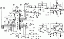
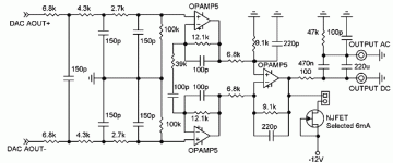
- Home
- Source & Line
- Digital Source
- CD6000OSE - tube output stage - help appreciated :-)