That's supposed to represent a constant current diode replacing the feed resistor for the reference LED.
Ah!
Thanks SY!
Of course... it should work better than just a resistor.
But how far should you go...
I think I will just use the resistor, the only CCS diodes I have easy access to are only rated 100V.
Thanks SY!
Of course... it should work better than just a resistor.
But how far should you go...
I think I will just use the resistor, the only CCS diodes I have easy access to are only rated 100V.
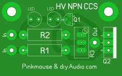
I think there is a minor error either on the NPN high voltage print board or on the schematic in post #6 in this thread.
On the NPN HV print boards (at least the batch I’ve got) the power transistor MJE340 is marked Q2, but in the schematic the MJE340 is marked Q1.
(The same error is done for the NPN low voltage circuit (Q1=Q2) but at here the transistors are the same type (BC549C))
Print board layout:
http://www.diyaudio.com/forums/attachment.php?s=&postid=829061&stamp=1138453582
Schematic:
http://www.diyaudio.com/forums/attachment.php?s=&postid=829231&stamp=1138481795
No problems - just a little bit confusing. 😉
Jan E Veiset
NO-6600
Tubehead said:... it should work better than just a resistor....
That's why I gave the option, the space was available and we wanted to make this PCB as flexible as possible.
Supply and return
For the NPN circuits, the supply connects to + and return to -
As I have seen some CCS connects supply to ground when return is negativ. Is this any different in this except for obviously voltages?
For the NPN circuits, the supply connects to + and return to -
As I have seen some CCS connects supply to ground when return is negativ. Is this any different in this except for obviously voltages?
jane said:I think there is a minor error
Thanx... that got caught earlier in the documentation, but until now it hadn't been fixed i that post.
dave
Correcting that las glitch got me to finsihing the changes to the documentation. We'll call this the public beta. Please let me know of any glitches or suggestions.
http://p10hifi.net/tlinespeakers/FAL/downloads/diyAudio-CCS-beta3.pdf [1.6 MB]
And a copy well written up examples from Gregg-the-Geek
http://p10hifi.net/tlinespeakers/FAL/downloads/AppNotes-0.2_HV_PNP_CCS.pdf [240 kB]
http://p10hifi.net/tlinespeakers/FAL/downloads/AppNotes-1.1_HV_PNP_CCS.pdf [268 kB]
dave
Dave,
What is the situation with (big)group buy lately?
I booked 5 sheets on the wiki a long time ago. Could you estimate cost + freight to Seoul, Korea? So that I can pay you by Master.
Thanks.
Kay
What is the situation with (big)group buy lately?
I booked 5 sheets on the wiki a long time ago. Could you estimate cost + freight to Seoul, Korea? So that I can pay you by Master.
Thanks.
Kay
It is time to move on this.
I'd like to get more comments from those that got proto-type boards.
Some of the comments i did get indicated that some board design would be worthwhile. The disadvantage of doing so would be a higher cost board.
A summary of the comments:
Pads are too small.
Holes are too small.
More versatility required for the variable resistor.
Be nice if the holes were plated thru.
Be nice if the real-estate the board takes up was smaller.
dave
Be nice if the real-estate the board takes up was smaller.
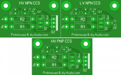
Just an idea. If you mirror everything the transistor can be rotated 180°. By doing this it can bend down to fix it to the chassis (cooling). The overall dimensions are 40mm by 25mm, for this size board two mounting hole are more than sufficient I think. I don't know if it is possible to do this setup with all the boards.
This is just a quick moving around of the parts, I don't know if Q1 is possioned correctly!
Regards
Attachments
Personally I don't see a need for plated thru holes because it makes it hell to remove a part if one needs to unless you have a desoldering station. I have (4) of them and I still don't like plated thru.
Why not one board that can do any of the three functions? Bigger holes don't hurt either for us older folk that don't see like we did when we were in our 40's.
Why not one board that can do any of the three functions? Bigger holes don't hurt either for us older folk that don't see like we did when we were in our 40's.
Bigger holes don't hurt either for us older folk that don't see like we did when we were in our 40's.
I'm still in my 40's.😀
Making one board to fullfill all three functions is going to lead to confusion I think.
Regards
Making one board to fullfill all three functions is going to lead to confusion I think.
We have good people here that are capable of making a good set of instructions.
The positive here is that the boards we purchase will get used up. Personally I would buy more knowing that I can use them all instead of having one type of board on my shelf because I never got around to using one for that function.
GeWa said:If you mirror everything the transistor can be rotated 180°. By doing this it can bend down to fix it to the chassis (cooling).
Morgan Jones advised me against this when suggested as it might lead to capacitive coupling and instability.
Morgan Jones advised me against this when suggested as it might lead to capacitive coupling and instability.
Are you reffering to the placement of Q2 against the chassis?
Why not one board that can do any of the three functions?
As far as I can see you can use the board for all three functions as long as you pay attention to the polarity of the LED's en the orientation and type of Q1 and type of Q2. For Q2 in the LV CCS you can just bend the legs a bit open.
Regards
GeWa said:Are you reffering to the placement of Q2 against the chassis?
Yes.
- Status
- Not open for further replies.
- Home
- Amplifiers
- Tubes / Valves
- CCS for tubes/valves: PCBs