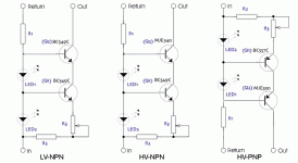
Having the transistor turned around would at least not having space on the board reserved for the heat sink (on those that require heatsinks). It would also give more heatsink flexibility.
And the idea of using 1 board for any of the 3 CCSs is one i like. Does mean good docs, but we want that anyway....
dave
And the idea of using 1 board for any of the 3 CCSs is one i like. Does mean good docs, but we want that anyway....
dave
Hi,
Tested. Only if a real crummy insulator is used with leads longer than 6". With a regular mica insulator, this isn't really an issue.
pinkmouse said:Morgan Jones advised me against this when suggested as it might lead to capacitive coupling and instability.
Tested. Only if a real crummy insulator is used with leads longer than 6". With a regular mica insulator, this isn't really an issue.
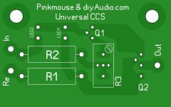

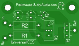
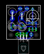
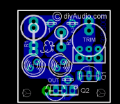
I didn't go over it for correctness, but suggest a few tweaks -- larger holes for variableR (geek -- where would the extra R go to fake the value of the cermet?), and some trimming of unused real-estate (light green bits), and room for a pink mouse next to the .com (all the PM icons i have have a mounting hole in them)
dave
dave
Attachments
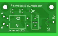
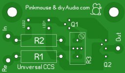
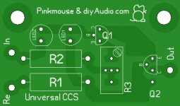
GeWa said:Dimensions are now 39mm x 23mm.
That is a 20% savings in real-estate. Means 6 boards fit where 5 used too (approx)
The only way to squeeze more out of the board would be to stand the Rs up... not pretty but effective. May be a bit more of a hazard thou with a couple live connections sticking straight up.
dave

Hi Dave,
One could just bridge it across the bottom pins. We have proven reliability for this in ChrisB's amp 🙂
planet10 said:(geek -- where would the extra R go to fake the value of the cermet?)
One could just bridge it across the bottom pins. We have proven reliability for this in ChrisB's amp 🙂
Greetings all,
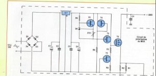
may I have your opinion on this design, it came from a french review LED which did not exist anymore. The author is J.Gest, but the second part of the article has never been published. Here is the component list also, but is missing the PCB layout.
R1=12 Ω 1/2W
R2=12 Ω 1/2W
R3, R4=33Ω 1/8W 5% if T2 and T3 2SK170BL
R3, R4=22Ω 1/8W 5% if T2 and T3 2SK170GR
R5=330 Ω 1/4W 1%
R6=7.5kΩ 1/2W
Rv1=5 kΩ 10 or 25 turns
C1=220 µF 35V 105°C
C2=220 nF 50V
C3=220 nF 50V
C4=22 µF 35V tantale goutte or CTS13
D1 to D4=1N4007
D5=TL 431
T1=BC549C
T2=2SK170GR or BL
T3=2SK170GR or BL
T4=2SK30AGR
T5=IRF840, IRF840AFI
IC1=7812
I'm currently trying to figure out the PCB layout, and I'm very bad for that...
Attachments
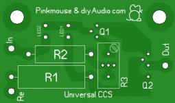
Well, I couldn't let GeWa have all the fun!
Yes, but does it have the fancy Pinkmouse logo? 😉
Regards
Come on, work in progress! 🙂
My mission is to leave absolutely no room on the board for the Advanced PCB logo that they stick on all their work.
Anyone for SMD?
My mission is to leave absolutely no room on the board for the Advanced PCB logo that they stick on all their work.
Anyone for SMD?
pinkmouse said:Anyone for SMD?
Not at this time...
But it wouls be interesting how small it could go...
dave
- Status
- Not open for further replies.
- Home
- Amplifiers
- Tubes / Valves
- CCS for tubes/valves: PCBs