Hi everyone.
I built the circuit several times using DN2540, and tried several different ones, and I can get down to 0.3 mA. No problem. Using different JFETs as the bottom device too.
I've read many times that a cascoded depletion mosfet CCS can be problematic if the Vgs of the top device is not large enough, as it limits Vds of the bottom device, and that limitis the minimum current that can be achieved.
Was I just lucky?
I just measured about -2.5V for the top device Vgs on one of those circuits I still have around, while set for around 0.4 mA.
Lingwendil,
Does the above still apply (dynamic Z lower at low mA) if the DN2540N3 is used instead? I'm unsure but I think the dies are the same in either package.
Not to derail the thread, as it's sort of on topic, but if I get a dynamic Z of around 2M with a BJT cascode, then what dynamic Z is considered low for a cascode DN2540 at these currents (<1mA)?
I have read that DN2540 likes 5mA or more current, but I havent tested yet (DN2540 arriving Monday)
I believe the main issue is that the dynamic impedance is much lower at lower current.
Yes, that's because Vds gets very small, and both input and output capacitances of mosfets increase a lot when Vds approaches zero.
But I recall reading people pointing that they were unable to reach a certain amount of current. What I don't know if that "unable" means "imposible to get there" or "unusable due to bad performance".
I know this topic of depletion mosfet CCS has been discussed many times in this forum, but after probaly an hour of seeking and reading I haven't found the answer to this particular question.
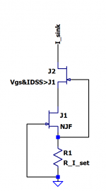
What is the voltage range over the cascode transistor?
The cascode JFET/depl-MOSFET should have higher IDSS and Vgs than the bottom device. As long as the bottom device has enough Vds, it will sink your current. There should not be a limit to how low current can be, rather there is a limit to how high it can be because the Vgs decreases as Ids increases, eventually not giving enough Vds for the lower device. But for many JFETs at <1mA the Vds can be <1V.
Place the gate of cascode as shown, not to GND.
Attachments
hi
For .3 ma maybe cascoded LND150 (500v to92) with
the low z mu output if your ccs is on the plate side.
For .3 ma maybe cascoded LND150 (500v to92) with
the low z mu output if your ccs is on the plate side.
Attachments
Last edited:
The cascode JFET/depl-MOSFET should have higher IDSS and Vgs than the bottom device. As long as the bottom device has enough Vds, it will sink your current. There should not be a limit to how low current can be,
Thanks for the added info. The upper limit was obvious to me, just looking at the curves, but it is the lower end what I still don't get.
Merlin wrote in one of his books about a cascoded CCS using DN2540: "[...] refuses to operate at the desired current no matter how much Rs is fiddle with [...] it was imposible to set the idle current to ~2.4mA [...] Rs was set arbitrarily at 470 ohm, yielding a current of 3.3mA".
What I understand from these words is that there seems to be a real unachievable limit.
For copyright reasons, I quoted the minimum possible amount of text, but I think that I didn't ignore any relevant detail.
hi
For .3 ma maybe cascoded LND150 (500v to92) with
the low z mu output if your ccs is on the plate side.
Yes, LND150 is clearly a better choice. The original question though is still there. What is the reason and implication of the lower bound?
There is no lower limit. Merlin must have had some feature/goal that set the limit.
Since you plan to cascode with a depletion MOSFET, use a JFET for the bottom device.
Looks like LN150 has IDSS of 1-3mA. So any JFET with IDSS < 1mA (max) will do. No problems making a CCS at < 100uA.
Since you plan to cascode with a depletion MOSFET, use a JFET for the bottom device.
Looks like LN150 has IDSS of 1-3mA. So any JFET with IDSS < 1mA (max) will do. No problems making a CCS at < 100uA.
Merlin wrote in one of his books about a cascoded CCS using DN2540: "[...] refuses to operate at the desired current no matter how much Rs is fiddle with [...] it was imposible to set the idle current to ~2.4mA [...] Rs was set arbitrarily at 470 ohm, yielding a current of 3.3mA".
Maybe I can make a guess at what happens here, though if Merlin still has this test setup in a drawer somewhere, the first suggestion would be: swap around the two FETs in the cascode.
To understand why this might matter start, as always, with the specification of the affected part.
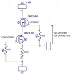
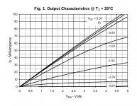
The relevant parameter is VGS(OFF). This is the gate-source voltage applied to the FET in order to reduce the drain current to 10µA (i.e. above the leakage current rating, but only just). It applies when the FET is operating in the pentode region since (VDS = 25V. Ha, yes, FETs have pentode and triode regions of their curves, which should present no problems to anyone here... but see the attached set of labelled curves (Oxner, 1982) to illustrate.
The upstairs FET is always in the pentode region, because the value of VDS is going to be above 20V in any reasonable application. Meanwhile the downstairs FET has to put up with a VDS of only the value of VGS of the upstairs FET.
Going back to the specification VGS(OFF): for DN2540 it is -1.5V to -3.5V. For the upstairs FET, in pentode region, this might mean a VGS of somewhere between about -1.3V and -3.2V for the upstairs FET, at a current of 3mA.
Since the upstairs FET might have simply been taken from the shipping tube without selection, we might have bad luck and get a FET with VGS(OFF) of -1.5V, meaning that the downstairs FET has to live with a VDS of only about 1.3V when the drain current is 3.3mA.
Now, let us suppose we had some more bad luck, and the downstairs FET has a VGS(OFF) of -3.5V. The gate-source voltage does not (of itself) matter to the downstairs position, but the more negative this value, the more likely we are to be operating the downstairs FET in the triode region (see picture). In the triode region, the drain current is dependent on VDS as well as VGS, and it is this that might raise some difficulty.
Merlin started with a DN2540 cascode running 3.3mA using a resistor of 470Ω. So VGS was -1.55V. We want it to run 2.4mA, so we might raise the value of Rs from 470Ω to 820Ω (say). Then, the downstairs FET tries to decrease the drain current, but as it does so, the upstairs FET forces its VGS more negative, to accomodate the lower current. Now, this greater magnitude of VGS is also the VDS of the downstairs FET. But, increasing VDS of a FET in the triode region acts to INCREASE the drain current!
- In other words, the upstairs FET fights any attempt to decrease the drain current, by forcing UP the VDS of the downstairs FET.
Sadly, the DN2540 data sheet curves are useless at low currents like these, so it is not obvious that the FET is in triode region at 3mA.
Instead, we can use the curves of a similarly-scaled FET to see the likely behaviour.
The IXTP10N100 is such a FET, and has just the kind of curves we need. And sure enough, it looks very triodey at VDS of 1.3-2.0V and 2-3mA.
The practical solution to the problem is simple enough: either select your DN2540s to have the upstairs part with high-magnitude VGS(OFF) compared to the downstairs; or use LND150 downstairs, as already suggested.
If you are not working with a cascode, there is no problem dialling in any arbitrarily low current value.
Attachments

Good explanation. Which is why:
'The cascode JFET/depl-MOSFET should have higher IDSS and Vgs than the bottom device.'
Was mentioned in my first post. I would chose a JFET for the bottom and a depl-MOSFET for tha cascode, if the voltage is > 25-30V.
Ideally the device chosen on the bottom should have Idss > 5 times the desired current for best regulation.
Yes, that is right! You can go even further, and say that the ideal choice of FET for the downstairs position will be one that will be operating in the pentode region at the desired current, and the voltage provided by the upstairs FET.
This is because the upstairs FET potentially gets hot, and heat drives VGS lower by 4.5mV/°C. Lower voltage for the downstairs means FETs in triode region will drift more than if they were in Pentode (saturated current) region.
If anyone really has an application for a 2mA current source (ECC83 anode load?) then another approach would be to replace the upstairs FET with a triode. A Russian 6П15П [6P15P] in triode at 100V will provide a VDS of about 9-12V for the downstairs FET - putting the downstairs FET into pentode mode AND reducing COSS by 60-85% at the same time. Perfect!
Excellent tip. How about using a pentode? Will it not give more compliance/dynamic range where the voltage can swing closer to the plate?
Edit: I guess now it gets complicated and if the voltage is to swing tens of volts and more we get into heater-cathode issues etc.
Edit2: If using a CCS as load on the bottom of a folded cascode or current mirror, where the CCS is to signal ground, and the plate is where the signal swings, I think a tube for the cascode device is very interesting.
Last edited:
Yes, a Penthode will make a hassle to feed the 2. Grid. Probably, the situation that makes most sense for triode-FET cascode CCS is where the voltage drop is high, as you say, current mirror. Or even anode-loads for low-current triodes, since the 120V or so drop in this case is better than many resistor options - and the performance will be in a different street.
The gate-source voltage does not (of itself) matter to the downstairs position, but the more negative this value, the more likely we are to be operating the downstairs FET in the triode region (see picture).
Excelent explanation. Thank you very much.
I suppose that devices with higher Vgs (that is, that require higher negative voltage to cut-off) have their curves "shifted upwards". Am I right? Else, I don't really understand why the statement I quoted above is true.
Good explanation. Which is why:
'The cascode JFET/depl-MOSFET should have higher IDSS and Vgs than the bottom device.'
Was mentioned in my first post. I would chose a JFET for the bottom and a depl-MOSFET for tha cascode, if the voltage is > 25-30V.
Ideally the device chosen on the bottom should have Idss > 5 times the desired current for best regulation.
Very useful too. I think I got it. Thank you.
Now that I have a better understanding, I'll go back to the bench and go deeper into the matter.


Excelent explanation. Thank you very much.
I suppose that devices with higher Vgs (that is, that require higher negative voltage to cut-off) have their curves "shifted upwards".
Yes, VGS(OFF) is just like an offset to the curves, at least from 10µA up to ca. 10mA.
The samples with greater-magnitude VGS(OFF) reach up to higher levels of IDSS, but that does not affect us in this discussion.
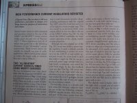
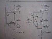
Walt Jung in the letters section of AudioXpress demonstrates a method to increase the Vds of the lower device in a MOSFET cascode CCS.
Thanks John. I had read this somewhere a few years ago, but my memory of it had vanished!
Do you think that that cascoded version using a pair of DN2540 would be a good choice for a current sink that will be used for ~75 volt drop at 6-10mA? I'm thinking of using that scheme for a tail under a 6N1P differential splitter, and already have a bunch of DN2540, but no other suitable depletion mode devices.
It should be workable, but may be worth making a quick rig that tests the value of VGS at the desired current. It's easy to do that by making up the Downstairs part of the circuit, and providing a 3-pin socket for the upstairs FET.
Plug the batch of FETs in the upstairs socket, one-by one; the best for upstairs duty will show the greatest magnitude of VGS of the upstairs position ( =downstairs VDS ) during the test. Those should give the least trouble from operating the downstairs FET in the triode region.
FETs are much more variable, sample-to-sample, than bipolar transistors, don't be surprised if some are very different to others in VGS.
Alternatively, you can use Walt's circuit, that John posted. That should solve the problem nicely, at the cost of the 1µF cap, and the two resistors.
I think I'll use Walts circuit from above, I have the extra parts on hand, and I need to build up a protoboard for the circuit anyway 🙂
Does the lower device need a heatsink for that version? I have a few TO92 DN2540 on hand, and was going to use them there if they don't need a heatsink. Otherwise I'll just do TO220 all around.
Does the lower device need a heatsink for that version? I have a few TO92 DN2540 on hand, and was going to use them there if they don't need a heatsink. Otherwise I'll just do TO220 all around.
- Home
- Amplifiers
- Tubes / Valves
- Cascoded DN2540 CCS down to 0.3 mA