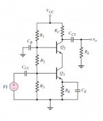
The Tektronix circuit is class A so It doesn't need a resistor for regulating thermal regime , just a zenner is enough there.Basically all the circuits are explained there in detail, the same with that RC network.Zener diode won't do it. The idea is to reduce Voltage across the lower device as it reaches max current to equalize power dissipation relative to the case where current tends towards zero at max Voltage. The lower device runs at nearly a constant temperature. Important when you have to make big square waves with flat tops and bottoms, typically with no feedback !
Just a guess, but I think R13 equalizes power dissipation through the signal range and C11 holds the Voltage constant above the frequency where thermal distortion is most troublesome. This paper was written in 1969 before Tek really hit their stride with the 7000 series. The 7000 series were state of the art lab scopes discontinued in the 80's.
I have to agree with you there. The idea is to limit Voltage across the output devices to stay out of the Second Breakdown zone. One of Nelson's patents shows a triple stack.
I suspect that modern transistors can solve a lot of problems that the old ones couldn't.I built many things ignoring protections with new components and barely had any problems unless i sent the probes on Mars 🙂
I would've wanted to put some pictures from Arto Kolinummi's book on audio amplifiers with the Candy variation of the bootstrap circuit too , but i'm not in good relationship with Linear Audio's owner and i don't want to risk being in need for a lawyer...if you have the book...page 238/239...
Last edited:
I have used the resistor between cascode and cascoded devices on
occasion, but it was to remove high frequency instability. I recall
commenting on this on the F5 turbo thread.
occasion, but it was to remove high frequency instability. I recall
commenting on this on the F5 turbo thread.
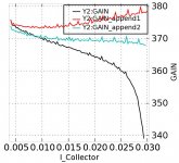
Here is a Toshiba 2SC2240 with gain curves plotted vs Ic. The curves from bottom to top are Vce of 3V, 4V, 5V. This particular part seems to be very linear at Vce of 4V at something like 15mA of bias.
I will cascode this part with either a BD139 or a TTC004B and plot some curves.
The cascode thing is starting to make sense.
I will cascode this part with either a BD139 or a TTC004B and plot some curves.
The cascode thing is starting to make sense.
Attachments
Wasn't there another topic about quasi saturation of bd139 /bc337 and ksc3503 transistors?
Yes, in the Solid State forum. I posted this here because I am interested in pursuing something similar to the Threshold amplifiers and I think it fits in the thread.
2N3904
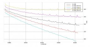
Here are the gain curves for a 2N3904. From bottom to top, Vce is 3V, 4V, 5V, 6V, 7V.
This transistor is nicely linear at 7V Vce if it is biased at 15 mA or so. The device is rated at 625mW at 25 deg C so it should be fine at 7V at 15mA.
The downside is that you chew up 7V of your rail.
If you want to do this without a curve tracer, you could build the cascode pair into a gain stage and measure the distortion. Tweak Vce of the gain transistor for minimum distortion. A perfect task for a DIYer.
Attachments
My own approach is to use a cascoded fet, as with the F3. The Vds
can be easily modulated against the rising transconductance to cancel
the bulk of the gain change.
can be easily modulated against the rising transconductance to cancel
the bulk of the gain change.
My own approach is to use a cascoded fet, as with the F3. The Vds
can be easily modulated against the rising transconductance to cancel
the bulk of the gain change.
Is that similar to what you did in the VAS of the AB100?
Attachments
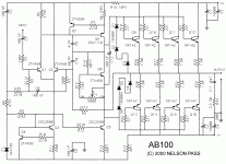
No, the VAS of the AB100 has no cascode. You'd want to read both the art_zv9.pdf and art_zv8.pdf for a clearer picture of what Papa said.
No, the VAS of the AB100 has no cascode. You'd want to read both the art_zv9.pdf and art_zv8.pdf for a clearer picture of what Papa said.
I was asking about gain modulation. Sorry if the question was not clear.
Does Q7 in the AB100 serve a similar purpose as Q4 in the F3?
Q7 is a current limiter.
Thank you for the explanation. Something new to learn for me.
Not complicated, when enough current flows through Q6, the voltage that
develops across R6 turns on transistor Q7 which drains the drive voltage
for Q6 which is seen across R5.

develops across R6 turns on transistor Q7 which drains the drive voltage
for Q6 which is seen across R5.
from the document art_zv8.pdf its given as ..
"The partner device, operated Common Gate, contributes so little of its own character to the output that it doesn’t rate as a gain stage per se, but it shields the actual gain device from the output voltage."
One question regarding this..
in cascode state, the main device (lower one) doesnot contributes much voltage gain and all the voltage gain is provided by the cascode device which is running in common gate/base mode. So how does the cascode device will not have its own character to output, as its providing most of voltage gain for the cascode stage.. could you please help understand this point ..
Also if we use high gain device like a BJT with high HFE as the cascode device, will the combined cascode stage will have more gain .. means can we use low gain JFET like 2sk246 and cascode with a BJT with high HFE and get a high combined gain for the cascode stage ?
- Home
- Amplifiers
- Pass Labs
- cascode output amp