Matt, thanks for that. But my purpose is a tracking notch that follows the oscillator as it wanders or drifts slightly. Say total tracking range of 6 to 10 Hz. For a nominal 1kHz oscillator that means it could vary between say 995 and 1005Hz and the notch, at nominally -40dB, will follow it and keep it centered. The goal, as you noted, is to decrease the ADC dynamic range requirements and thus its distortion.
A flat notch with a similar width would be nice but the ones I found were always 4 or more staggered notches and pretty complex. The tracking is not that hard to do, but the issue is the distortion from the tuning system. It is much easier though than the AGC of an oscillator because the control speed can be very slow (oscillators typically drift over 10's of seconds or even minutes) and there is almost total absence of oscillator signal in the control signal. The remaining non-linearity is the inherent non-linearity of a tuneable impedance.
Jan
Hi Jan,
An alternative to the tunable Bainter notch would be a state variable filter notch that can be tuned a few Hz one way or the other without degrading the notch. This could be implemented by putting a variable resistance JFET in series with each integrator resistor, with its source at the virtual ground of the integrator op amp.
This JFET can still benefit from the use of 1/2 of the drain signal as feedback to its gate. In an application where you only need to move a few Hz, the voltage that needs to be across the JFET will be quite small, so very little distortion will be introduced.
Note that the gain of both integrators must be changed so that the gains of the integrators remain the same; else the notch will be degraded. Although the Bainter can in principle provide a deeper notch without tweaking, if you do not need a super deep notch, the SVF notch may work well for you.
Cheers,
Bob
I was not sure, if a person is real. Would you think, an author should instantly recognize his own creature? And if it didn't happen?The author of that article is a member here and has already posted in this thread ;-)
I believe those resistors are for stability reasons. I have used my GP opamp implementations with wildly unequal input resistances and they were clean down to -160dBc.
There is something else going on here.
I will be away a few days but intend to test the cap to ground.
Jan
Regarding input matching, I'd refer to OP275 DS
https://www.analog.com/media/en/technical-documentation/data-sheets/OP275.pdf
Know, they are talking JFET, nevertheless BJT has similar C-B capacitance, and it's easier to cancel a variable in THD equation by matching impedance. Certainly, could be more than one reason for high THD level.Attention to Source Impedances Minimizes Distortion
Since the OP275 is a very low distortion amplifier, careful attention should be given to source impedances seen by both inputs.
As with many FET-type amplifiers, the p-channel JFETs in the
OP275’s input stage exhibit a gate-to-source capacitance that varies with the applied input voltage. In an inverting configuration,
the inverting input is held at a virtual ground and, as such, does
not vary with input voltage. Thus, since the gate-to-source voltage
is constant, there is no distortion due to input capacitance modulation. In noninverting applications, however, the gate-to-source
voltage is not constant. The resulting capacitance modulation
can cause distortion above 1 kHz if the input impedance is
greater than 2 k and unbalanced.
I now believe that the 20 ohms made a difference because it made the notch less deep which also means that the internal voltages, especially at the output of the opamp driving R1, also drop, which would lead to the lower distortion.
The difference was only a few dB anyway.
Jan
The difference was only a few dB anyway.
Jan
Know, they are talking JFET, nevertheless BJT has similar C-B capacitance, and it's easier to cancel a variable in THD equation by matching impedance. Certainly, could be more than one reason for high THD level.
As I mentioned, the circuit I posted only uses inverting mode stages thus this effect does not apply.
Jan
I now believe that the 20 ohms made a difference because it made the notch less deep which also means that the internal voltages, especially at the output of the opamp driving R1, also drop, which would lead to the lower distortion.
The difference was only a few dB anyway.
Jan
That would de-Qing the capacitor which should show up in a simulation.
Hi Jan,
I wonder if distortion might be improved slightly if the GP3 stage were moved so that it drives input to R3, akin to https://www.analog.com/media/en/training-seminars/tutorials/MT-203.pdf There would be some attention of distortion and noise by the GP2 integrator stage.
Just a thought...
I wonder if distortion might be improved slightly if the GP3 stage were moved so that it drives input to R3, akin to https://www.analog.com/media/en/training-seminars/tutorials/MT-203.pdf There would be some attention of distortion and noise by the GP2 integrator stage.
Just a thought...
That would de-Qing the capacitor which should show up in a simulation.
It does. Those 20R resistors decrease the notch dept from over 60dB to about 40dB. And it lowers the signal voltage at the output of the integrator by several dB. That could explain the difference in distortion, more than the 20R decoupling the capacitive load.
I was kind of stuck in this rut, I think I should stop worrying about that cap load and move on with the design.
That resistor R1 that I use for tuning is actually a trimmer on my protoboard. I will replace it with a fixed metal film to see if that makes a difference, but that will have to wait a few days as I am at the beach taking a Corona-break ;-)
Jan
Jan since the Bainter notch still requires correction at 2H and 3H what is its advantage over the Hall notch which has a one resistor control?
The advantage is that I know the Bainter and never heard from the Hall notch ;-)
I will look it up.
BTW You can fix the Bainter such that it doesn't require correction for H2 and H3 (or at least only a few tenths of a dB).
Jan
I will look it up.
BTW You can fix the Bainter such that it doesn't require correction for H2 and H3 (or at least only a few tenths of a dB).
Jan
Hi Jan,
I wonder if distortion might be improved slightly if the GP3 stage were moved so that it drives input to R3, akin to https://www.analog.com/media/en/training-seminars/tutorials/MT-203.pdf There would be some attention of distortion and noise by the GP2 integrator stage.
Just a thought...
Actually I specifically moved GP3 to that position so that the cap drive would be isolated from the (unknown, often) source impedance.
Jan
The advantage is that I know the Bainter and never heard from the Hall notch ;-)
I will look it up.
BTW You can fix the Bainter such that it doesn't require correction for H2 and H3 (or at least only a few tenths of a dB).
Jan
Hank's note shows how to make it asymmetrical I think.
I found a thread here about the Hall notch, where halfway someone promoted the Bainter over the Hall as much easier tuned. Go figure ;-)
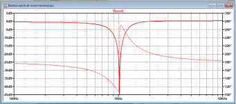
Bainter with flat 2nd - 3rd response.
Jan
Bainter with flat 2nd - 3rd response.
Jan
Attachments
Last edited:
I found a thread here about the Hall notch, where halfway someone promoted the Bainter over the Hall as much easier tuned. Go figure ;-)
Bainter with flat 2nd - 3rd response.
Jan
I found Bainter's original article, Hank left out a few steps and has an error. I see now how to tune it.
but the issue is the distortion from the tuning system.
You might think about the the CdS + LED (NSL-32S42) that Jim Williams used in his 2011 article--it works really well. The voltage across the CdS is very small (10-20 mV), the distortions of the oscillator are well under -140 dBC. Plus, the control is simple and 100% isolated--a DAC and opamp with 10-20 mA of drive capability could do the trick.
I indeed am using the NLS-32 .... And that 20mV is indeed a sweet spot. You're no longer allowed to guess here 😎
Jan
Jan
Re -135 HD. We need to put this into perspective to see what could cause it. -135 dB is around 300 parts per billion, a very small number. for a 32 nF cap 1 ppm would be 32 fF so this is around 10 fF equivalent change in capacitance somewhere. Its very conceivable that the input C is modulating that much with even the small voltage at the inverting input. The input C change varies a lot in different amp circuits. A cascoded circuit will have less modulation. It usually shows as odd order (if I have it right) since its a single ended phenomena, except on complementary inputs where it could be symmetrical.
When you are looking at nonlinearity this low everything will show up. PCB, solder mask flux residue and component issues can all show up. Lower impedance helps until current effects show up. A classic demo with the CLT-1 is to take a pencil lead to a resistor lead on a resistor under test. it increases the distortion as the lead interacts with the magnetic field around the wire.
When you are looking at nonlinearity this low everything will show up. PCB, solder mask flux residue and component issues can all show up. Lower impedance helps until current effects show up. A classic demo with the CLT-1 is to take a pencil lead to a resistor lead on a resistor under test. it increases the distortion as the lead interacts with the magnetic field around the wire.
Re -135 HD. We need to put this into perspective to see what could cause it. -135 dB is around 300 parts per billion, a very small number. for a 32 nF cap 1 ppm would be 32 fF so this is around 10 fF equivalent change in capacitance somewhere. Its very conceivable that the input C is modulating that much with even the small voltage at the inverting input. The input C change varies a lot in different amp circuits.
An input charge error should show up in a simple resistive inverter circuit, the capacitor only shifts the phase 90 degrees. The composite amp IIRC has enormous AOL at 1kHz, I can only extrapolate from the paper but there should be <micro-Volts at the input.
Yes. Samuel's best guess is that the distortion at 1kHz is about -200dB (his measurement limit was -180dB). The OL gain is gigantic at 1kHz. Microvolts at most as differential input signal. It find it very hard to imagine that this would modulate the input capacitance.
It will be some days before I am back home and can experiment again, but my suspicion now is the trimmer that is in R1 position.
Jan
It will be some days before I am back home and can experiment again, but my suspicion now is the trimmer that is in R1 position.
Jan
Bainter's original article, Electronics, october 2, 1975 :
https://www.google.com/url?sa=t&rct...inter%29.pdf&usg=AOvVaw0MP32i0c89qUT3WCgfXMJK
Bainter "How to Write Node Equations for Active Circuits" :
https://www.google.com/url?sa=t&rct...s/MT-203.pdf&usg=AOvVaw39cMM10Qdeka8nRmzHwI1k
Zumbahlen "Bainter notch filters" :
https://www.google.com/url?sa=t&rct...s/MT-203.pdf&usg=AOvVaw39cMM10Qdeka8nRmzHwI1k
Last edited:
- Home
- Design & Build
- Equipment & Tools
- Capacitive load impact on distortion