I don't know how to measure Vp, so I can't help you there. However, how can you have DC offset when the circuit uses 10uf electrolytic capacitors AFTER each buffer stage? Even the balanced version has a 10uF cap for the + and the - of the circuit.dc offset 0.7Vdc but when I changed to 2SK170 gr its dc offset go down to 0.01Vdc.
Thanks again, Bill. I will try again to trace the circuit, but am having a hard time. I will take your advice and complete populating the SUB section. I just need to find the key place to "unplug" the SUB section and the SUB GAIN section as I will not be using that channel.It's not the HOW, it's the WHO that matched them. Nelson Pass supplies all the matched JFET's with resistors, all of the resistors for the JFET's are the same. You can install the JFET's and resistors since they are all the same in any position on the PCB you want.
That will leave only the R1,R2,C1, C2 answer, there you might need to use an ohmmeter to trace the PCB to the schematic. Do one at a time and double / triple check your results. Don't assume the positions are the same for each section of the PCB, trace each sections R1,R2,C1 &C2.
Don't forget to finish the SUB section, the PCB fully completed now is better than finding out someday you want to add a SUB and can't find the parts to complete.
Thanks Nelson. While pondering the schematic, if you also have any advice about how best to remove or jumper over the SUB, SUB GAIN or WOOF HI PASS sections, please post.
I measured dc offset at the center of top and bottom jfets buffer.I don't know how to measure Vp, so I can't help you there. However, how can you have DC offset when the circuit uses 10uf electrolytic capacitors AFTER each buffer stage? Even the balanced version has a 10uF cap for the + and the - of the circuit.
Need help in solving offset at T2 test points.
I purchased the matched JFETs and resistors from LinkWitz.store and completed assembling the board.
The voltages between the test points T0 and T1 show about 1.24v.
The voltage at T2 varies throughout the board. In the attached PDF, sections marked as BAL INPUT, OUTPUT INV, and SUB GAIN the voltage at point T2 varies between -100 mv to +200mv. In the sections marked as LO PASS, the voltage is around 2.4 volts; in all the other sections, the voltage is around 1.24 volts.
The SMPS output is +15.3v and -14.5v, after the power supply filter section where it is marked as - and + 14v, the voltages are +14.3 and -13.5 volts.
Frank confirmed the voltages at test point T1 look right and asked to check the component values for T2. I have measured all the resistors and checked the PCB a few times for dry solder, and shorts.
Any pointers would really help.
Attachments
Hello @Nelson Pass, could you please suggest what could be wrong? I have been talking to Frank and he mentioned he never saw issues around T2 test points.
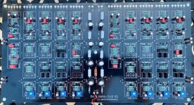
The interesting thing is, I am getting the exact incorrect voltage on both left and right at the positions I mentioned in my previous post. I have attached the picture of the assembled PCB.
Thanks.
The interesting thing is, I am getting the exact incorrect voltage on both left and right at the positions I mentioned in my previous post. I have attached the picture of the assembled PCB.
Thanks.
Attachments
Hello Subbu -- I wish I could help. I continue to monitor this space. Meanwhile I have a mostly completed board, and 6 amplifiers all hooked up and waiting to be fed by an active crossover. Without a schematic or some assist from the seller or designer there is little we can do! I found Frank to be non-helpful. And there's been nothing from Nelson Pass since early June, when he said he would "look at it tomorrow". But we never heard from him. We evidently have an orphaned Nelson Pass design that we cannot make work because there is no schematic, no support from the seller, and little interest from the designer. Surely at least a schematic exists?
what you got and could get from Nelson is based on his good will and volition, same as everything he does here
what you paid and (by your words) didn't get proper support for, that's completely different - certainly not Nelson's commercial product
so, wait for Pa's free time, but you can't think him being accountable
what you paid and (by your words) didn't get proper support for, that's completely different - certainly not Nelson's commercial product
so, wait for Pa's free time, but you can't think him being accountable
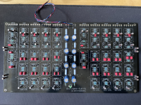
Hello Subbu and others -- I have attached a pic of my board. It's not a great pic and I can do close ups if needed. But the pic shows my overall progress thus far. I feel I am SO close, but need one bit of information to complete. Again I am adapting this crossover for use with my 3-way Spendors. So you can see in the pic the areas where I have mounted connectors so that I can easily change values of Cs and Rs to tweak crossover slopes if needed. I have determined the values of the Cs and Rs using the calculator that is online. The calculator identifies these as C1, C2, R1, R2 and which 'box' (i.e. MID Lo Pass or FR Hi Pass etc.) is known. The missing link is what positions within each box correspond to C1, C2, R1 and R2. Can anyone help?
Attachments
@Zen Mod I understand the points you are making. I have been a member here for many years and this is the first time I have asked for help. I have no need to pin accountability on Nelson Pass. That is up to him. I look at this forum as a place where people like me can get help just as you might ask for help from friends. Of course a friend does not act out of 'accountability' they act out of a desire to help. Nelson may be the only one who can help and he graciously offered his help on a couple of occasions in this thread. If a friend of mine agrees to help and then gives me unusable help, and then offers to help again and then does not, I am disappointed in my friend. I am not saying Nelson Pass is a friend of mine, only that I thought this forum offered help on a similar basis. So am I disappointed? Yes. Should that be a surprise?
all I'm saying is that I fully understand you, but I'm also understanding Nelson; he is one and there are many of us, expecting and getting
You could take it upon yourself to trace out the circuit by examining the board and drawing the schematic. There are plenty of well documented and related crossover schematics that you can refer to for comparison. When you bought the board you made certain assumptions as to its applicability to your application. Rather than waiting for help that may or may not materialize, you could notch up your level of effort and figure it out.
Actually Frank contacted me and I gave him a response. The DC offset at T2 is not a real issue. The buffer circuits use a follower which has no Source resistor and those Jfets are run at currents lower than Idss, so they have a little offset which places a small DC bias on coupling caps. In the low pass filters this adds up but is not a significant issue as it is removed before the output.Hello @Nelson Pass, could you please suggest what could be wrong? I have been talking to Frank and he mentioned he never saw issues around T2 test points.
The interesting thing is, I am getting the exact incorrect voltage on both left and right at the positions I mentioned in my previous post. I have attached the picture of the assembled PCB.
Thanks.
Thank you for your inspiring character advice but I am a big boy and do have my big boy pants on. And have actually "taken upon myself" to reverse into a schematic by tracing the board. Not sure if you have even seen this board but I myself have never before "taken it upon myself" to try to trace a circuit this complex. And I have traced many a circuit in my long life (but I must admit never a fully balanced active preamp, usually tube amps, tube preamps or power supplies). So my bad, I will "notch up my effort" and I am sure if I can only overcome my character flaws all will be fine. No. Not really. You see, I did "notch up my effort" and still could not figure it out. So rather then banging their head against the wall, what to do? Smart people look for advice. Hence here we are. Oh and BTW I may be ignorant IRT this particular board, but I am not irresponsible, stupid or lazy.You could take it upon yourself to trace out the circuit by examining the board and drawing the schematic. There are plenty of well documented and related crossover schematics that you can refer to for comparison. When you bought the board you made certain assumptions as to its applicability to your application. Rather than waiting for help that may or may not materialize, you could notch up your level of effort and figure it out.
That's good to know, @Nelson Pass . Would appreciate if you could respond about that issue you were reading up on back on June 5 I refer to in post #50, above. In short I just need to know what positions within each box correspond to C1, C2, R1 and R2. Barring that, even just posting the schematic would be a great help.Actually Frank contacted me and I gave him a response. The DC offset at T2 is not a real issue. The buffer circuits use a follower which has no Source resistor and those Jfets are run at currents lower than Idss, so they have a little offset which places a small DC bias on coupling caps. In the low pass filters this adds up but is not a significant issue as it is removed before the output.
In short I just need to know what positions within each box correspond to C1, C2, R1 and R2. Barring that, even just posting the schematic would be a great help.
Rob -
What you are asking for is probably NOT something Nelson can do for you. Your project is not a PASS LABS, FRISTWATT, nor PASSDIY product. He has sold his designs to others since the 70's (maybe earlier), as with most business transactions, he probably doesn't have the rights to the schematic, nor the PCB blueprint which you so desire for C1, C2, etc. location on the PCB.
In regards to what to do with the SUB & SUB Gain, don't do anything except not use them or get a SUB and use them. No harm will come either way.
As far as locating correct placement of components, in your case the low and high filter parts, I've already sent you the schematic for the filters, all you have to do is find the placement for C1 OR C2. Once you found one of them, the other is obvious. It will also make the placement for the resistors fall in your lap based on C1 and/or C2 location. By the way, every low pass and high pass filter parts location on the PCB is the same for every section (low, middle, high,SUB etc.).
As I hadn't heard from you since June, I figured you had this solved and were listening to music. You only have an hours worth of work to finish it, find a time when no one is around to bother you and go find WALDO (C1 or C2).
Bill
Hi - Good to hear from you. Don't worry, I wasn't working away on this problem for the past 3 or 4 months. And I do have music, using one channel of each three-channel amp to loop back thru the old passive crossovers.
I took several attempts at tracing the circuit. Was able to identify and sketch out the power side. But when it came to signal it had me stumped and probably as frustrated as I've been, doing DIY audio for the past 50 years. That was the same time that Nelson Pass seemed to indicate he would come back with some additional information. And the same time some serious health issues took center stage and I did not have the bandwidth for more conundrums. So it was time to take a pause.
It probably will seem strange to you, but thinking back, this may be the first time I've had to trace a purely SS circuit! I know how a tube works and what has to flow in and out of it to make it work. Hand me a tube board or schematic and all I do is look for that triode symbol and the rest falls into place. Maybe the dedicated solid state folks on this forum have a similar SS frame of reference that makes simple work of tracing this board?
Knowing little about how commercial arrangements are made, you could be right, Nelson Pass does not have the information that would help, but he seemed to indicate that he does. I do know that Frank (at Linkwitz Audio) related some frustration that he could not get a schematic from Pass. And my board is prominently marked (C) 2019 Passworks. And I always thought that (C) indicates where the intellectual property is owned and resides.
Your info "...every low pass and high pass filter parts location on the PCB is the same for every section (low, middle, high, SUB etc.)" is very helpful. And thanks again for ALL your help and your encouragement. Hopefully my health issues will resolve. When they do I will persevere and will figure it out. Certainly not "waiting around" for Mr. Pass to follow thru as the presumptuous fellow above admonished me for doing. I know better, and actually have more important things to deal with.
I do hope I can PM you in future, if only to say hi. But as hero worship and receiving reprimands from a fairy-like surrogate are not my thing, I think I'm gonna take a break from this forum for awhile. All the best to you Bill.
Rob,
Since I have some familiarity with this board I can mention a couple of things that should be understood.
First, it is not "fully differential." There are circuits at the input and output to convert to/from single ended from/to differential. (You may be confused by discussion of the LXMIni crossover which suggested that for differential operation a duplicate circuit is required.) The active filters are not differential, but single ended.
Second, for a three way crossover you need the SUB channel, the MID channel and the FR. WOOF and FR are used for a two way crossover. SUB has second order lowpass and some equalization required for the +2 sub in the original (intended) application. The MID channel has both a highness filter, to align with the lowpass of the SUB channel, and a lowpass filter which aligns with the highness filter of the FR channel.
I do hope I can PM you in future, if only to say hi.
When your ready, PM me and I'll show you how to find the C1 location, I've never traced a complete PCB either, I never will. Life is to short.

- Home
- Amplifiers
- Pass Labs
- Can you help me to modify crossover points on a Balanced LXMini Crossover?