@Citizen124032
Hello, good night, master, when I connect R68 to ground, not to the output, all frequencies before 20kz remain at 0 Db, so I did not change the R68 resistor.
The test results that I can understand and do are already above.
According to the topology and the test results I have done, I have not found a significant problem for now (of course, since there are not every component in the proteus program I use, I tried to test it with components with approximate values.
You can download the latest version of proteus ub from this address
https://www.fullindir.cafe/proteus-professional-full-indir/
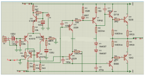
I'm already actively using the amplificador circuit in the link, I can say that by making a small addition to this circuit, I added R66 and R67, as well as Q37 and Q38 Components.
http://www.videorockola.com/proyect...tencia/amplificador-estereo-400w-version-2-0/
Hello, good night, master, when I connect R68 to ground, not to the output, all frequencies before 20kz remain at 0 Db, so I did not change the R68 resistor.
The test results that I can understand and do are already above.
According to the topology and the test results I have done, I have not found a significant problem for now (of course, since there are not every component in the proteus program I use, I tried to test it with components with approximate values.
You can download the latest version of proteus ub from this address
https://www.fullindir.cafe/proteus-professional-full-indir/
I'm already actively using the amplificador circuit in the link, I can say that by making a small addition to this circuit, I added R66 and R67, as well as Q37 and Q38 Components.
http://www.videorockola.com/proyect...tencia/amplificador-estereo-400w-version-2-0/
Last edited:
I downloaded the program you said by your master, but it will take a long time to learn itYou need to use LTspice. Your amp is actually "olde English" , the Spanish master copied it.
The LT version of this amp is posted. Actually , very clean for this simple amp. .01% at 20k. NICE !
The 2 files (.asc + the cordell models) go in the same folder. Sim will run good.
This is a good topology to build ..... Q6/7/8 can be mje340/350... any ??? on my extra additions or component choices ,
feel free to ask.
Go to https://www.analog.com/en/design-center/design-tools-and-calculators/ltspice-simulator.html best stuff !!
"Well forged designs" he he he !! Like Badgers and Wolverines ?
I referred to R68 in #15, also known as R7 (68k) in the OP, or R25 (100k) in #17....when I connect R68 to ground, not to the output, all frequencies before 20kz remain at 0 Db...
The feedback resistor not connected to the output, but to ground to make it an open loop amplifier.
Attenuate the input signal with the feedback factor (open loop gain / closed loop gain) to get approximately the same output voltages.
Disconnect R68 / R69 / Q35 from the output altogether: no feedback!
I estimate the open loop gain at 16000x (very roughly), so the attenuation should be 16000/68 (#1!) = 235x.
Given a supply of +/-50Vdc, max output is (100/3=) 33Vac -> max input signal is 33 / 235 = 140mVac.
Start with 10mVac, see what it does at 100mVac if no clipping occurs.
Post the open loop gain Bode plot (gain & phase!).
Calculators are for freshman.
Attachments
Post scriptum:
If the dc setpoint of the output node (5200-1943) runs away, add a 1kΩ res between the 330Ω and the two bias diodes to tie it near supply midpoint; +/-5Vdc at output is allowed here because we're interested in the ac openloop gain behaviour only.
Do the simu again with a 8Ω load and a speaker-alike load.
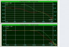
here are the new results, the top two graphs belong to the new drawing
before the bottom two graphic changes
but now I have the opportunity to test live by applying this change on the amp that I actively use.
there is no device like an oscilloscope so I will have tested it according to my own ear

before the bottom two graphic changes
but now I have the opportunity to test live by applying this change on the amp that I actively use.
there is no device like an oscilloscope so I will have tested it according to my own ear
I’m not sure quite what you are trying to say here - bode plots are generated with an AC simulation, and that doesn’t ‘understand’ anything about signal levels. It simply linearises every device at the DC operating point, so 100-volts input will still show 50dB gain if that is what the small-signal gain is.Disconnect R68 / R69 / Q35 from the output altogether: no feedback!
I estimate the open loop gain at 16000x (very roughly), so the attenuation should be 16000/68 (#1!) = 235x.
Given a supply of +/-50Vdc, max output is (100/3=) 33Vac -> max input signal is 33 / 235 = 140mVac.
Start with 10mVac, see what it does at 100mVac if no clipping occurs.
Post the open loop gain Bode plot (gain & phase!).
Calculators are for freshman.
For a transient simulation, 100mV (peak) at the input will certainly drive the input diff. pair into hard compression, 10mV should be fine for the first diff. pair, but the second one will probably still be clipping.
The amp that I am actively using in my daily life has almost the same design as the one in the diagram, but all I have to do is connect the output end of the 68k resistor to ground to make the change you mentioned.Add the plots hereafter.
Don't run a real amp in open loop unless it is designed to do so!!!
I apologize that I do not fully understand some of the terms you use.
I'm sorry, because I use translation and my knowledge of electronic terms is weak, I did not understand much from what you wrote.I’m not sure quite what you are trying to say here - bode plots are generated with an AC simulation, and that doesn’t ‘understand’ anything about signal levels. It simply linearises every device at the DC operating point, so 100-volts input will still show 50dB gain if that is what the small-signal gain is.
For a transient simulation, 100mV (peak) at the input will certainly drive the input diff. pair into hard compression, 10mV should be fine for the first diff. pair, but the second one will probably still be clipping.
@Citizen124032
I just disconnected the R68 resistor as you said and connected it to ground and I powered the amp for a second, as a result, an incredible sound came out from the speakers in the form of bo bo bo bo bo bo bo
As a result, it is absolutely wrong to Separating the R68 resistor from Out!!!!
I just disconnected the R68 resistor as you said and connected it to ground and I powered the amp for a second, as a result, an incredible sound came out from the speakers in the form of bo bo bo bo bo bo bo
As a result, it is absolutely wrong to Separating the R68 resistor from Out!!!!
In the upper Bode plot the open loop turn over is at 2kHz, but more important the pole around 30kHz which causes the peaking in the closed loop!here are the new results, the top two graphs belong to the new drawing
before the bottom two graphic changes
I suspect the first stage differential here - a RC between the collector legs might supress it (4k7/100p).
Phase is -130° and gain is +6dB at 1MHz, just nearing instability even at a -20dB/decade slope.
Also seen in the closed loop where the phase is -90°/decade from 70kHz onwards.
With a gain of 16dB at 1MHz (same phase), there might occur oscillation at 2MHz.
Attachments
Read my remark at #29 (again):I just disconnected the R68 resistor as you said and connected it to ground and I powered the amp for a second, as a result, an incredible sound came out from the speakers in the form of bo bo bo bo bo bo bo
Don't run a real amp in open loop unless it is designed to do so!!!
My comments were directed towards Citizen24032, as he appears to be confusing how an AC simulation works, and over estimating the linear range of a differential pair.I'm sorry, because I use translation and my knowledge of electronic terms is weak, I did not understand much from what you wrote.
Taking a step back, I think there is an error in how the bias for the input transistors is drawn. I’m guessing the intention is to use Q32 as a capacitance multiplier. In this case, R50 should be between the supply and the zener, R58 should be between the zener and Q32 base. Q32 collector should be connected to the supply. (all references are for the schematic in post 15). I think what you have at the moment will work as a relaxation oscillator, giving the ‘Bo-bo-Bo’result you report With the built amplifier.
It appears to me that the circuit around D9-Q32 acts as a voltage regulator to ensure a very constant current through R49 (33k). Hence my remark in #16.
I'm not sure if the amp behaved as a relax oscillator - it was in open loop.
I'm using Spice as a simulator, but do not distinguish ac from dc states actually to understand what's happening really in an amp.
Not the Occam's razor method, but the superposition view.
I'm not sure if the amp behaved as a relax oscillator - it was in open loop.
I'm using Spice as a simulator, but do not distinguish ac from dc states actually to understand what's happening really in an amp.
Not the Occam's razor method, but the superposition view.
Parts added to the original schematic in #1 failed in real life so I went back to the original schematic the only change was edited to a complementary pair of PNP-NPN instead of a pair of NPNs
The problem right now is that the schematic has 2 transistors, so it has an 8ohm output, but the speakers I have are 4 ohms. I'm looking for a way to solve this problem.
The problem right now is that the schematic has 2 transistors, so it has an 8ohm output, but the speakers I have are 4 ohms. I'm looking for a way to solve this problem.
This script of simulations to test the circuit is very interesting. It will also be useful for me, because I know that, to test a circuit, there are simulations to be done but I couldn't say which ones they were.Current source (R49, 33k) from a regulated supply is very unusual, maybe not neccessary. Curious and unique though.
Cascode with R66-R67 can inject ripple from the negative rail - a current source from the rail will prevent that.
There is no HF compensation in the first stage - it might oscillate.
C18, C19 are miller cap's for Q30, Q33, but is this the right way / the proper values? The BJT's are on the edge.
Q30 is the counter for Q1, but very different. Is Q1 fit for the supply voltage? See remarks #3.
Bias setting with D11, D12 and R60 is very simple, but not very reliable, and with temperature drifting Q29-Q34 will drift too.
The VAS must run on 42mA at least to hop over class B setting, which is very high.
I doubt the values of C17 and C20 - calculations or proof needed.
Add a resistor of >100k on the connector side of C22 to prevent pops when connecting a source.
Zobel network.
HF compensation over R68.
Add values of node voltages and collector currents from the simulations to the circuit diagram for better understanding.
Run a dc analysis injected on the base of Q36 and see if things remain stable.
Run a ac analysis from sub frequency up to 10MHz, a Bode plot (dB and phase) and absolute voltages and currents if all values fits the specs of the components.
Run an ac open loop gain analysis (R68 not connected to the output but to ground), with reduced level (obvious) and observe the behaviour of the amp, especially the higher frequencies. A Bode plot shows hidden zero's and most important hidden poles!
Run if possible a transient analysis.
Run a dc supply start-up & shut-down analysis - is the amp stable during these transits or is destruction looming
Do a power supply analysis - what is needed (voltage, current, caps, bleeders, bridge current peaks, transformer performance, mains filtering).
Do a PSRR analysis - what amount of supply ripple will be injected where and how much and how to reduce it.
Make a plan for a build, wiring, component placing, grounding, safety, ventilation & heat sinks, operability, transportablity, EMC behaviour.
Just to address a few.
Hopefully it sounds a bit decent. But that's only known after all the effort has been done.
There was another circuit involved too, not?
Same issues.
But I wish you well, good luck with the design and above all: a lot of fun and pleasure!
- Home
- Amplifiers
- Solid State
- Can Transistor Amplifier Experts Help?