good day ,
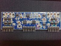
I am repairing a Cadence ZRS C1 mono car amp, i found out no signal to 1 bank of the amplifier section that is why the audio is very weak. Can you please provide the IC numbers of U2 and U3 in the picture of board driver of the mosfet in the amp. section. U1 chip is readable but U2 and U3 i believe was burnt out. Thank you in advance.
I am repairing a Cadence ZRS C1 mono car amp, i found out no signal to 1 bank of the amplifier section that is why the audio is very weak. Can you please provide the IC numbers of U2 and U3 in the picture of board driver of the mosfet in the amp. section. U1 chip is readable but U2 and U3 i believe was burnt out. Thank you in advance.
Attachments
Last edited:
They are a TL072 and an LM211. The LM211 has pins 1 and 4 directly connected.
The transistors along the top of the board (7, 11, 19 and 22) commonly fail, as well as the 470 ohm resistors near them,
The transistors along the top of the board (7, 11, 19 and 22) commonly fail, as well as the 470 ohm resistors near them,
Thank you very much Perry, it is a big help for me. I will purchase the parts and get back to you as soon as possible of the progress of the repair. More power bro.
Hi Perry, i got the SMD parts, but i did not fixed it yet because i found out that R24 in the picture circled with red was blown also and the markings are erased. Can you please provide me the value of the resistor or mark in it. Thank very much as always with your help.
Attachments
As always, thank you very much Perry. I will post you the progress of the repair. I am planning to purchase the Repair Tutorial by next month, is there an easier way to download it. Like, you can just e-mail me the Zip file? Thanks.
There is no easier way. It's 4G+. Email me if you have any other questions about the tutorial. I don't want to contaminate the thread.
babin_perry@yahoo.com
babin_perry@yahoo.com
Good day bro, is there anybody who has the schematic diagram of this amp Cadence ZRS C1 mono amp. will be a big help for me in troubleshooting. Thank you so much.
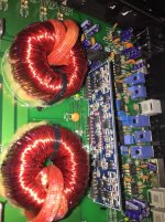
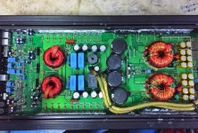
The Driver board and ouput mosfets (10 in each bank) where removed then I checked the rail voltage on the FETS, I was surprised, why am i getting no rail voltage on the Drains holes but i am getting positive rail voltage on the Gate and Source on the 5 FETs which i believe the HI side and Negative rail voltage on the Gate and Source on the other 5 FETs which i believe is the Lo side. But as far as i know correct me if im wrong, in the Hi side there should be no voltage on the Gate and Source but with positive rail voltage on the Drain and in the Lo side should be Negative rail voltage on the Gate and Source with no voltage on the Drain. But why i am not getting the positive rail voltage on the HI side drains? Does this amp have a different design ? Please enlightened me, I'm just confused.
Attachments
- Home
- General Interest
- Car Audio
- Cadence ZRS C1 mono amp