If done like the data sheet suggests it will work, and will likely damage the chip.
Should have read: ... will NOT work,...
I'm still not following. What would happen if, say, i used an 50V X7R here? The capacitance would be all sorts of voltage dependent, but how would that ruin my day?Ceramic capacitor are not very linear nor noise free when voltages near their rated voltage. You should always use ceramic capacitor with 10 times (4 times minimum) the voltage rating required in every case where the capacitor is in the direct signal path (bootstrap capacitors are in the direct output signal path).
EDIT: I get that an X7R is going to be really non-linear when biased near it's max voltage, but i don't get why linearity is really needed here. The bootstrap pins probably don't behave any sort of linearly.
I also recommend using the FAULTZ pull-up connection of MUTE as described in the data sheet. Although the data sheet is completely wrong in how it's actually done. If done like the data sheet suggests it will work, and will likely damage the chip. Do it as it's done in the eval board instead.
You're talking about the weirdness on page 19 in the datasheet? Still, why can't i just short MUTE to ground? I don't intend to short the outputs for extended periods of time.
Last edited:
Updated: https://github.com/rosvall/tpa3132-amp
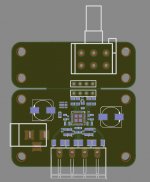
This does feel less cargo cult. Star ground, every return path is clear. Nothing on top layer goes under the ferrite beads.
I'm keeping the input ferrite beads for now. I really hate those cable clip-on things.
How does it look to you?
Also, i feel kind of bad coming of so arrogant in my previous responses. It's not that i'm doubting you, i just really want to know the hows and whys. I'd like to get an intuition for this stuff.
Last edited:
Couple thoughts...
1. ADD 1210 x 2 bypass Caps (each side). Remove the 0805 stuff. The 1210 has the same ESL as a 0805. You can bypass with all the 0.1uf caps you like and it will not make a difference. High di/dt -> dv/dt.
2. REMOVE the FB on the ground. Changing the impendance on the ground plane is not going to help the noise issue.
3. The Main Power routing is too long and too narrow. Increase track width and shorten the distance. Route the Signal lines on the back side so the Power can be routed straight across.
4. I very much doubt you will be able to solder the TPA3132 to the PCB without wicking all the solder down those vias....plus the via density is too high. you need more surface area. You need to switch to the TPA3116. much easier to hand build.
5. Keep the snubbers on the chip side and remove post FB snubbers. You need to relax on the EMI / RF issues. You have them covered.
Dwight
Last edited:
I need to read up on MLCC SMD caps. I don't quite get why their datasheets don't have any ESL or ESR figures.Couple thoughts...
1. ADD 1210 x 2 bypass Caps (each side). Remove the 0805 stuff. The 1210 has the same ESL as a 0805. You can bypass with all the 0.1uf caps you like and it will not make a difference. High di/dt -> dv/dt
It wouldn't help with common mode noise?2. REMOVE the FB on the ground. Changing the impendance on the ground plane is not going to help the noise issue.
Done! I think that part looks much better now.3. The Main Power routing is too long and too narrow. Increase track width and shorten the distance. Route the Signal lines on the back side so the Power can be routed straight across.
I've removed some of the vias. I do imagine it's going to a pain in the *** to put this thing together, but i like the awesome compactness of the QFN. Also, i think it's more elegant to use the ground plane as heat sink, than some clumsily mounted alu profile. Somewhere, probably in the tpa3116d2 thread, Saturnus mentioned mounting the backside of a board directly to a case/heat sink. I quite like that idea, even if it would require some annoying SMD connectors.4. I very much doubt you will be able to solder the TPA3132 to the PCB without wicking all the solder down those vias....plus the via density is too high. you need more surface area. You need to switch to the TPA3116. much easier to hand build.
Anyway, at the moment my plan for soldering it involves a toaster oven and a syringe of solder paste, and probably a lot of swearing 🙂
I do want to have them covered. The trouble is that i'm really ignorant and would rather be safe than sorry. I need to figure out how to calculate how much filtering is really needed.5. Keep the snubbers on the chip side and remove post FB snubbers. You need to relax on the EMI / RF issues. You have them covered.
Dwight
In any case, thanks for taking the time. I appreciate it. I feel like this thread is really making me smarter, even if it might seem like an uphill battle for you guys.
OK ROSVALL,
I see we are making progress... Strong Work on removing the FB on the GROUND 😉
Couple thoughts...
1) Given the current size of 31 mm x 38 mm , you only need two mounting points. You will need the space for the issue in #2.
2) The routing for C6/C7 is weak... The caps are 'bypassed' by the current routing The routing needs to go 'across the pad'.
3) The FB traces needs to be wider... seriously use some copper. 🤐... The Trace from the FB to the Supply trace is absolutely lame... Go Big or Go Home.
4) I see you have narrowed the Supply tracks again... See #3
5) Any Chance of a 1210 ?? or is it ??
??
5) Final thought for the evening.... You are dumping all the heat into the GND plane. Any plans to remove it ?? The PCB's limited heat capacity is going to become very when you turn the volume up.
Dwight
https://github.com/rosvall/tpa3132-amp/blob/master/tpa3132-amp.pcb.composite.png
I see we are making progress... Strong Work on removing the FB on the GROUND 😉
Couple thoughts...
1) Given the current size of 31 mm x 38 mm , you only need two mounting points. You will need the space for the issue in #2.
2) The routing for C6/C7 is weak...
The caps are 'bypassed' by the current routing The routing needs to go 'across the pad'. 3) The FB traces needs to be wider... seriously use some copper. 🤐... The Trace from the FB to the Supply trace is absolutely lame...
Go Big or Go Home. 4) I see you have narrowed the Supply tracks again... See #3
5) Any Chance of a 1210 ?? or is it
?? 5) Final thought for the evening.... You are dumping all the heat into the GND plane. Any plans to remove it ?? The PCB's limited heat capacity is going to become very
when you turn the volume up. Dwight
https://github.com/rosvall/tpa3132-amp/blob/master/tpa3132-amp.pcb.composite.png
Last edited:
Heh, thanks.OK ROSVALL,
I see we are making progress... Strong Work on removing the FB on the GROUND 😉
Couple thoughts...
You're right. It's a bit sloppy.1) Given the current size of 31 mm x 38 mm , you only need two mounting points. You will need the space for the issue in #2.
2) The routing for C6/C7 is weak...
Duly noted.3) The FB traces needs to be wider... seriously use some copper. 🤐... The Trace from the FB to the Supply trace is absolutely lame...
I admit they it's a bit thin and sad looking, but it's only supposed to carry like 2-3A.4) I see you have narrowed the Supply tracks again... See #3
It's coming, i've just not yet found a cap that i like. And i still haven't found any specific figures on ESL and ESR, which bugs me. I'd like to at least be able to pretend to make an informed choice based on some numbers.5) Any Chance of a 1210 ?? or is it
The idea (that i've stolen from Saturnus) is to mount the board on some sort of heat sink. I've still to find some appropriate SMD connectors to make that possible though.5) Final thought for the evening.... You are dumping all the heat into the GND plane. Any plans to remove it ?? The PCB's limited heat capacity is going to become very
Dwight
https://github.com/rosvall/tpa3132-amp/blob/master/tpa3132-amp.pcb.composite.png
I suppose that, if i'm using this thing as an amp for a 2-way speaker, the power output to the tweeter is much smaller than for the woofer. And in any case, playing at top volume with VCC=25V, a crest factor of 5 and 15% loss, it should generate less than
(25V)^2/8Ohm/2 * 1/5 * 15% * 2channels = 2.4W of heat
Which is still way too much for that tiny-*** board, but it doesn't require a lot of heat sinking. When only one channel is playing the low frequencies, and with less compressed music, we're talking something like 1W. That's almost doable without a heat sink.
The thermal resistance from junction to ground plane is about
5.5 + 400/16 = 31 degC/W
Total for small board:
31 + 1000/(3.1*3.9) = 114 degC/W
For a 50x50mm board:
31 + 1000/(5*5) = 71 degC/W
I think i could improve those figures a bit by using bigger vias.
At the moment i'm trying to fit an ADAU1761 DSP and an MCU on the board. That's a big part of the reason for squeezing everything together and using some 0603 parts. I want it all to fit on a 50x50mm board. I'll post an update when/if it's done.
The idea (that i've stolen from Saturnus) is to mount the board on some sort of heat sink. I've still to find some appropriate SMD connectors to make that possible though.
Double adhesive isolating thermal tape is the obvious answer. If the whole bottom side of the PCB is a ground plane there will be more than enough thermal transfer.
I suppose that, if i'm using this thing as an amp for a 2-way speaker, the power output to the tweeter is much smaller than for the woofer. And in any case, playing at top volume with VCC=25V, a crest factor of 5 and 15% loss, it should generate less than
(25V)^2/8Ohm/2 * 1/5 * 15% * 2channels = 2.4W of heat
Which is still way too much for that tiny-*** board, but it doesn't require a lot of heat sinking. When only one channel is playing the low frequencies, and with less compressed music, we're talking something like 1W. That's almost doable without a heat sink.
Where does the 2 come in? Crest factor is average level under peak. Not average level under RMS. So what you're actually describing is with a crest factor of 10.
Note that this chip should not be supplied with much more than the 19V recommended. Please refer to figure 7 in the data sheet to find the efficiency at the average music level. To me it looks closer to 22% loss than 15% loss (19V; 8ohm; 4.5Wavg). So the absolute maximum heat sink dump is:
2 * 19^2/8 * 0.1 * 0.22 = 2W
I think i could improve those figures a bit by using bigger vias.
Use the 9 via hole pattern suggested in the data sheet. Alternatively, you could use 4 very large vias instead.
At the moment i'm trying to fit an ADAU1761 DSP and an MCU on the board. That's a big part of the reason for squeezing everything together and using some 0603 parts. I want it all to fit on a 50x50mm board. I'll post an update when/if it's done.
If you're going to have multiple supply voltages available anyway then I suggest splitting the AVCC and PVCC rails completely, and run the AVCC rail of a 5V supply. This is because a large portion of the idle losses in the TPA3132 is due to losses in the internal LDO. It will also completely eliminate PVCC fluctuations from affecting the digital and analog circuits.
Last edited:
I stock some on my table and can miss three of them if you are interested ;-)Damn, it doesn't look like anyone stocks the NJU7181 and i can't figure out what to search for to get an alternative.
Hi all,
anyone considered additional filtering for the AVCC part? Datasheet + EV-Manual suggests just to connect directly to PVCC. Looking into the datasheet, the interal LDO is ~-60dB CMRR up to 20kHz. Would an LC-filter improve this in some way?
Regards,
doc
anyone considered additional filtering for the AVCC part? Datasheet + EV-Manual suggests just to connect directly to PVCC. Looking into the datasheet, the interal LDO is ~-60dB CMRR up to 20kHz. Would an LC-filter improve this in some way?
Regards,
doc
Hi all,
anyone considered additional filtering for the AVCC part? Datasheet + EV-Manual suggests just to connect directly to PVCC. Looking into the datasheet, the interal LDO is ~-60dB CMRR up to 20kHz. Would an LC-filter improve this in some way?
Regards,
doc
Even a simple ferrite bead between the PVDD and AVDD improves sound so I'd imagine it also measures better. Just remember AVDD has to be within 0.5V of PVDD.
No ideas really. But it has severe stability issues if outside +-0.5V of PVCC.
Since that is the exact same voltage variation range of GVDD I imagine it might have something to do with that. Possibly the internal dc/dc converter ratio for GVDD is referenced to PVCC but supplied by AVCC. As GVDD can be higher than supply voltage it's probably not an LDO supplying it directly even though the schematic implies it. But that's just guessing.
Since that is the exact same voltage variation range of GVDD I imagine it might have something to do with that. Possibly the internal dc/dc converter ratio for GVDD is referenced to PVCC but supplied by AVCC. As GVDD can be higher than supply voltage it's probably not an LDO supplying it directly even though the schematic implies it. But that's just guessing.
I wouldnt say, GVDD could be higher than supply-voltage.
Datasheet states 6.9V for AVCC=PVCC=7.4-26V
With AVCC=PVCC < 7.4V, i would rather think that GVDD is dropping as well (Vdrop ~500mV).
Datasheet states 6.9V for AVCC=PVCC=7.4-26V
With AVCC=PVCC < 7.4V, i would rather think that GVDD is dropping as well (Vdrop ~500mV).
I wouldnt say, GVDD could be higher than supply-voltage.
Datasheet states 6.9V for AVCC=PVCC=7.4-26V
With AVCC=PVCC < 7.4V, i would rather think that GVDD is dropping as well (Vdrop ~500mV).
Supply voltage can be 4.5V to 26V though.
I know, but if GVDD could be higher than PVCC, they would have specified, don't you think?
I'm going to evaluate this.
Datasheet states 6.9V for AVCC=PVCC=7.4-26V
I'm going to evaluate this.
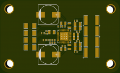
Placement of core components within 50x32mm (fitting DP5032 case):

Of course, power-paths needs to get polygonized and alot of via stitching needs to be done. (Beside adding connectors)
Of course, power-paths needs to get polygonized and alot of via stitching needs to be done. (Beside adding connectors)
Attachments
Last edited:
Attachments
- Status
- Not open for further replies.
- Home
- Amplifiers
- Class D
- Building a TPA3132 amp board