Oh nice! Way smaller than I thought 🙂
How is it most effectively installed? Each winding in series to the output of a channel (left/right)? Or a winding in series to a channel and the other in series to the HPs' GND? In the second case I would need two, one for each channel.
I wonder also if the HPs GND would need its own choke, since in the current circuit it is a +5V VGND.
If the HPs are balanced then its quite easy - you'll have 4 wires so one side of the CM choke goes in series with each wire. One choke for L, another for R. If your HPs are 3 wire then its a bit more tricky, I guess put the two GND (in your case GND=mid rail) side inductors in parallel.
I hope that the following drawing interprets you well (one channel).
I'm wondering also if the VGND circuit needs protection as well. I don't know much about electromagnetism, but since the VGND output is at a considerably higher voltage than GND, I imagine that EMI could interfere between the headphones GND wire (VGND) and the device's chassis (GND). If that's plausible, would for example a small capacitor between GND and VGND be of any use or needed (see drawing)? Problem is that the opamp can't be loaded with capacitance without a series resistor, then EMI will take the least resistant path into the opamp's feedback loop. 🤔
I'm wondering also if the VGND circuit needs protection as well. I don't know much about electromagnetism, but since the VGND output is at a considerably higher voltage than GND, I imagine that EMI could interfere between the headphones GND wire (VGND) and the device's chassis (GND). If that's plausible, would for example a small capacitor between GND and VGND be of any use or needed (see drawing)? Problem is that the opamp can't be loaded with capacitance without a series resistor, then EMI will take the least resistant path into the opamp's feedback loop. 🤔
Attachments
Since its RF we're talking about here then C1 can be sized to have negligible effect at audio frequencies so I'd reduce it to 2.2nF then it'll be ~100X higher impedance than your 32ohm load at 20kHz. You could add the same on the driven output to provide a preferential route for RF to GND. Make R8 a bit bigger (say 22R) so as not to degrade the phase margin of the opamp too much.
I'm tempted to add single series inductors on the opamp outputs too for 'belt and braces' but so far haven't found a suitable part.
Yes your diagram interpreted my intentions for the CM choke but seems to have lost a cap (at the output of the DAC) in transcription from my pic.
I'm tempted to add single series inductors on the opamp outputs too for 'belt and braces' but so far haven't found a suitable part.
Yes your diagram interpreted my intentions for the CM choke but seems to have lost a cap (at the output of the DAC) in transcription from my pic.
Yes, that's the right idea. If you fancy going the whole hog then these inductors might give some benefit between the opamp output and the RC network just added : https://www.mouser.com/ProductDetail/TDK/ADL3225VT-4R7M-TL000?qs=yB%2BpDD7iBPVPDn/0tfqvRg==. But perhaps try it to see how the RF rejection is with just the CM choke first. If the opamp stability turns out to be compromised by the RCs, reduce the caps to 220pF as even that low value is going to give a degree of RF rejection.

Great! That's perfect. I'll try this out first on PCB. It will take me a while though to update other sections on my system.
I may want to introduce some gain to the signal for (64ohm) headphones that, under certain circumstances in which ambient noise is high or the source signal too low, are happier in my experience with 4Vpp. I'm not sure yet if this would be better done rising the digital signal or including 1.3Av gain (3K / 1K) to the opamp's feedback loop. The second would destroy the filter curve you created though. And maybe add some distortion, so I might better leave like this. The DACs will be powered with 5.6V so they should handle 4Vpp fine I guess.
I may want to introduce some gain to the signal for (64ohm) headphones that, under certain circumstances in which ambient noise is high or the source signal too low, are happier in my experience with 4Vpp. I'm not sure yet if this would be better done rising the digital signal or including 1.3Av gain (3K / 1K) to the opamp's feedback loop. The second would destroy the filter curve you created though. And maybe add some distortion, so I might better leave like this. The DACs will be powered with 5.6V so they should handle 4Vpp fine I guess.
I think you can add 6dB of gain to the opamps and reduce the feedback cap by a factor of 2 and still have a nice filter curve. Let me try it in LTSpice and report back. If your HPs are 4-wire rather than 3-wire you can drive them balanced at the cost of doubling up the DAC/LC filter circuits. But you'll only need one extra OPA1622, not two.
Yes on 5.5V supply the DAC's output swing can be 4Vp-p with the right choice of I/V resistor.
Yes on 5.5V supply the DAC's output swing can be 4Vp-p with the right choice of I/V resistor.
My headphones are unbalanced and wouldn't like to change that atm really, for versatility and especially because footprint is very crucial here. But why the need of extra opamps for the extra gain? I had something like this in mind–gain within the opamp filter. But the nice flat filter curve is now gone.
Here is my sim and OPA1622.lib, if you like: https://www.dropbox.com/scl/fi/bmuk...ey=khcqfrl966xz9anhhaexhhxjp&st=i03jjn1r&dl=0

Here is my sim and OPA1622.lib, if you like: https://www.dropbox.com/scl/fi/bmuk...ey=khcqfrl966xz9anhhaexhhxjp&st=i03jjn1r&dl=0
No need of an extra opamp just to add gain, the extra opamp's needed for balanced which also, as a side-effect adds 6dB gain. According to my sims C9 reduced to 1.2n gets the response flat again with your extra 2.5dB gain.
It is so relieving to have you help on this, other than fiddling myself with values alone.
After all I think the most 'elegant' solution (not that I consider elegant myself) would be to increase the IV resistors a bit to get the 6dB needed (4V) out of the DAC. This would save me 4 resistors on the board also. So IV resistors increased to 1.8k, keeping the standard values for capacitors you chose before. The response seems to remain quite flat.
I plan to keep the VREF pins of the DACs floating. I remember it being your preferred setup for bass response and it saves a lot of space, but I hope that's fine also with a fast ARM in the neighborhood.
Then I'm a bit sceptic about piggyback, after building a 20chip tower that ringed a lot unless I soldered along many ceramics for VCC decoupling. So this time I'm thinking to have each chip on the board with a ceramic each one. A correct value I suppose would be 27n (4x27n=108n), plus a 1000uF cap common to all chips. All powered by a CSS with 5.6V zener. A fine master plan?
I wouldn't bother with dividing the decoupler value in 4, just stick 100nF on each. On my multiple-paralleled DACs I don't have a decoupler per chip though I use bigger than 100nF. But if you have the room on the PCB, why not?
I found C2 = 6.2nF gave a more classic response with the increased I/V resistor values. Other than that, all looks fine. Incidentally, where did the 0.00228 amplitude of the current source come from? That's because you're running the 1387s at 5.6V supply?
I found C2 = 6.2nF gave a more classic response with the increased I/V resistor values. Other than that, all looks fine. Incidentally, where did the 0.00228 amplitude of the current source come from? That's because you're running the 1387s at 5.6V supply?
When I had ringing problems, it seemed to me that only 100n decouplers would stop it effectively. When I tried bigger values, supposing them to be more effective, ringing came back; the same when chose values significantly lower than 100n. Seemed like magic to me, as if the chip is made to be decoupled with that value, but I'd be fine if that was circumstantial and this makes no sense in general.I wouldn't bother with dividing the decoupler value in 4
Yes. The datasheet shows a max of 1.14mA, I guess that being at the max. rated voltage of 5.5V. As far as I remember this is peak-to-peak amplitude, whereas Spice works with peak amplitude, so for 4 chips I wrote 2.28mA only. I might be mistaken if you see noticed something there.where did the 0.00228 amplitude of the current source come from? That's because you're running the 1387s at 5.6V supply?
I asked about the current source amplitude because I'd like to simulate the circuit in the time domain to check that the DAC output compliance voltage isn't exceeded in the worst case. The LC filter doesn't present a purely resistive load to the DAC, particularly close to the corner frequency where its input impedance becomes strongly reactive. Its around there that the compliance might be exceeded for high level signals.
I think your math for the peak amplitude is fine. Incidentally you can always tweak up the output current a bit on TDA1387 if needed, with a resistor from pin7 to pin5. It does gain you a bit in ultimate SNR, maybe 1 or 2dB but it also makes the chip run hotter.
Here's the time domain result - the compliance is slightly exceeded but I suspect real music won't have such energetic high frequency content so likely everything is fine. Green is the filter input, magenta the output.
Last edited:
Thanks very generous from you Richard. Let's call that approved design 'chumingoOPA' for any further reference 🙂
I've been tinkering with the OPA1622 and it sounds precise but very representative. In the sense that the sound is thin and distant, not physical and strong like a transistor based amp–or taking the output directly from the DACs for that matter. I know these are subjective descriptions, but I wonder if there is any reasonable explanation for this other than test bench differences and personal bias. Or differences in THD.
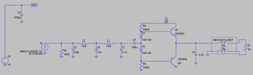
In the skepticism and need to compare I started simulating an alternative discrete AB version (AB for low consumption), adding an extra LCR stage to make the reconstruction filter curve similar to the OPA version. Actually the footprint is not that bigger that the OPA and I reckon it might sound more punchy and direct. Or again, more distorted simply? Surely more minimal. Below a reference image of the topology I'm thinking about, if there is anything exciting about it.
I've been tinkering with the OPA1622 and it sounds precise but very representative. In the sense that the sound is thin and distant, not physical and strong like a transistor based amp–or taking the output directly from the DACs for that matter. I know these are subjective descriptions, but I wonder if there is any reasonable explanation for this other than test bench differences and personal bias. Or differences in THD.
In the skepticism and need to compare I started simulating an alternative discrete AB version (AB for low consumption), adding an extra LCR stage to make the reconstruction filter curve similar to the OPA version. Actually the footprint is not that bigger that the OPA and I reckon it might sound more punchy and direct. Or again, more distorted simply? Surely more minimal. Below a reference image of the topology I'm thinking about, if there is anything exciting about it.
Attachments
So the subjective verdict is - that the OPA1622s don't deliver such a satisfying experience as going direct from the I/V resistors? That has been my normal experience in playing around with DACs - for example my Kubelik DAC design had some very nice opamps (OPA2209) acting as I/V stage and filer, but those were beaten fairly convincingly on dynamics and realism by some bipolars acting as unity gain followers. My hypothesis is that the opamps were noisier than the discrete transistors but in reality those opamps are almost as low noise as they come (2nV/rtHz input noise). But I don't have a better hypothesis. OPA1622 is a little bit noisier than OPA2209 but not by much.
I think you could get quite a lot of enjoyment from your proposed discrete stage, its similar to a buffer I made many years ago which sounded great even though it likely had crossover distortion. It was a diamond buffer made out of darlington transistors as I wanted high input impedance. Here your input impedance can be quite low, coming from the I/V resistor so you could experiment with a 'stock' diamond buffer. The difference is that the diodes on yours are replaced with transistors (emitter followers). You can use 2N3904/6 again.
Incidentally your second stage LC probably will need a termination resistor with those component values. I just went to Markimicrowave and the 20kHz 5th order LP filter without termination at the output looks like this :

OK so I did put in a termination R, it doesn't change the values much at all if you increase it to 500k.
I think you could get quite a lot of enjoyment from your proposed discrete stage, its similar to a buffer I made many years ago which sounded great even though it likely had crossover distortion. It was a diamond buffer made out of darlington transistors as I wanted high input impedance. Here your input impedance can be quite low, coming from the I/V resistor so you could experiment with a 'stock' diamond buffer. The difference is that the diodes on yours are replaced with transistors (emitter followers). You can use 2N3904/6 again.
Incidentally your second stage LC probably will need a termination resistor with those component values. I just went to Markimicrowave and the 20kHz 5th order LP filter without termination at the output looks like this :
OK so I did put in a termination R, it doesn't change the values much at all if you increase it to 500k.
Hey @abraxalito!
No I didn't have the chance yet to try the OPA1622 directly on the TDA1387, mostly because the only OPA1622 I have are already soldered on an AKM DAC board I'm using currently. My comment was regarding a comparison between a TDA1387(4x) + JLH1969 compared to this AK4384 + OPA1622–what I have at hand right now. Both sound very different and I think it's mostly because of the amplifiers, one being discrete (JLH) and the other a very powerful opamp. My feeling is that, even though the OPA is supposed to have enough output current, the JLH beats it in terms of realism; it is like being surrounded by and inside the sound space, instead of being in front of it–at a distance. Opamps have a lot of negative feedback, maybe it's that, but there are many opamps before in my system. Or maybe that my JLH is 2Vrms, or that it has a lot more current readily available, or that it is class A. It is difficult to tell with such different systems, might be even the DACs. I tend to blame the output stage (discrete bipolars vs powerful opamp) because I once tried a TDA1387 stack with an AB transistor output current buffer similar to the one shown before. It sounded pretty close to my JLH. Maybe even a normal opamp driving discrete bipolars in AB configuration would sound better than the OPA1622, because of more low-speed current availability. Don't you think?
I have fond memories of plugging the headphones directly to the 24x TDA1387 I-outputs also, but THD was really high without reconstruction filter. I could clearly hear images sweeping down with a 20-20kHz sweep test. Power consumption was very high and ripple injection probably too, without some massive power supply decoupling somehow.
Did you ever published your diamond AB buffer for headphones? I'm curious about it. Still I'm trying to find the optimal setup for my system, with minimal footprint, extreme low power supply ripple injection (to protect nearby preamps) and high current output. Looking forward to the have the time and parts to try different possibilities and what we've sketched the other day (chumingoOPA).
I'm also curious about how ripple injection is normally handled, as mentioned I have so preamps sharing power supply. Most information around deals with cleaning the power supply so ripple doesn't affect the amplifier. But not much on how to avoid the amplifier polluting the power supply. The most obvious way for me would be introducing a small resistor between a big decoupling cap and the amp's power supply, at the cost of increasing the power supply impedance of course. Or using a capacitance multiplier.
Cheers,
Domingo
Hey @abraxalito,
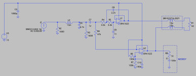
I'm doing a shopping list to build the OPA schematic in post #191. In post #180 you suggest the Bourns SRF4532TA choke for EMI protection at the buffer's output. You show there a graph of the SRF4532TA-601Y as the highest Z version, with an impedance of 1K at 500MHz. But the datasheet has a second page that maybe you didn't notice, where the highest Z version is actually the SRF4532TA-282Y with an impedance of 1K at 100MHz. This might be beneficial for a more robust protection to radios I guess, but the downside is higher DCR (0.35ohm) and lower max. current (0.9mA). My load is not higher than 100mA, but I'm not sure if this overhead is good enough, the upgrade justified or if you would still recommend the highest impedance version have you noticed them all.
I'm doing a shopping list to build the OPA schematic in post #191. In post #180 you suggest the Bourns SRF4532TA choke for EMI protection at the buffer's output. You show there a graph of the SRF4532TA-601Y as the highest Z version, with an impedance of 1K at 500MHz. But the datasheet has a second page that maybe you didn't notice, where the highest Z version is actually the SRF4532TA-282Y with an impedance of 1K at 100MHz. This might be beneficial for a more robust protection to radios I guess, but the downside is higher DCR (0.35ohm) and lower max. current (0.9mA). My load is not higher than 100mA, but I'm not sure if this overhead is good enough, the upgrade justified or if you would still recommend the highest impedance version have you noticed them all.
I took a look at the other plots that it looks like I missed for some reason and didn't much like the look of the -282 version as it has a kink around 1.8GHz which is a mobile phone frequency. So I would go for the next one down, -142. That also has a very decent max current capability and a low enough DCR.
I've been working on the design in post #191 and found out two design problems. One is that the input bias current of the OPA1622 is high and produces a lot of DC offset at the output in this configuration. Enough to be problematic in a DC coupled design like this one. The OPA2156 seems to solve that.
The other major problem is that this was meant for unbalanced headphones, so virtual grounds would be tied together. Each virtual ground is an opamp output, meaning the outputs would be shorted. Having series resistors between them would increase the impedance of the headphones ground... I'm thinking I might need some current buffer ICs now 🤔
The other major problem is that this was meant for unbalanced headphones, so virtual grounds would be tied together. Each virtual ground is an opamp output, meaning the outputs would be shorted. Having series resistors between them would increase the impedance of the headphones ground... I'm thinking I might need some current buffer ICs now 🤔
- Home
- Source & Line
- Digital Line Level
- Building a portable I2S 4x TDA1387 DAC