I am working on an ADC and DAC design with the aim to get a very good performance, suitable for testing audio systems. Right now I am looking at AKM's AK5394A for the ADC and the AK4399 for the DAC.
Later on I might want to try the ES9102 and ES9018/9018K2M.
I have made designs with the CS5381 and CS4398. They certainly show a good performance, but some of the design constraints in that project (supply voltages and op-amp choices) limit the performance in some respects.
I want to make a modular design, so that the analog input and output parts are on separate PCB's, so that I can change the design of one part without having to do the whole thing every time. I do plan to include the buffer in front of the ADC on the same PCB as the ADC though.
I have made an isolator and master clock design for the MiniDSP USBStreamer.
http://www.diyaudio.com/forums/digital-source/244042-master-clock-isolator-minidsp-usbstreamer.html
This design is working fine and I expect to use this for the interface to the PC. Sample rates are expected to be 48kHz and 192kHz. And perhaps I will include also the 44.1kHz based sample rates, so that I get all the "usual" sample rates up to 192kHz. At the moment I am not aiming for higher sample frequencies.
For the interface between the analog front end and the ADC I would like to use a fully differential, DC coupled interface with relatively large signal levels, to reduce the potential noise problems. Depending on the analog front-end design this may be optimized later, by eliminating one buffer stage, but at the moment I would like to have the flexible, modular design.
Something like the OPA1632 or the LME49724 could probably be used here. I hope that I can get a distortion and noise performance of the buffer, which does not degrade the performance of the ADC or at least only marginally. Not just at 1 kHz, but also at higher frequencies. Even if I should switch to the ES9102 and assuming that they can keep their specified THD+N level of -118 to -120dB.
Does anyone here have experience with the real life performance of the OPA1632 versus the LME49724?
Another option I consider is to make a "Birt circuit" (or "Superbal"), similar to what is shown e.g. in the THAT Corporation
http://www.thatcorp.com/datashts/De-integrating_Integrated_Circuit_Preamps.pdf
page 35. It would at least allow a broader selection of op-amps.
Has anyone tried this? Any good or bad experiences with this circuit? The op-amps could e.g. be OPA1612 or LME49990. Or perhaps the AD797.
JensH
I want to encourage this project as much as I can.
I have been thinking about the analog interface problem since you sent the PM to me. Let me outline the issues so the magnitude of the problem is clear-
1) Signal to noise ratio needs to be greater than an AK5394A in all expected modes, that means 123 dB or more. (the detailed definition of this is more complex)
2) Distortion products must all be less that -115 dB
3) High common mode rejection differential input, so you get only the signal you want.
4) differential out symmetrical around the midpoint
5) High input impedance so it doesn't affect the source
6) Input induced nonlinearity needs to be very low so it doesn't add distortion to high impedance sources
The signal to noise requirements dictate high voltages and low impedances. The max P_P voltage on the input is 2.4V for each input or 4.8V P-P (1.7V RMS) differentially for FS out. The noise needs to be-124 or more dB below this. The distortion should also be less than this if possible.
AKM uses a simple 3 opamp solution that relies on either a good differential source or using an opamp to make a single ended source into a differential out (inverter). While this works it does not have much common mode rejection and requires active intervention to go from differential to single ended.
Circuits like the THAT differential design are low impedance input and require very close matched resistors (On the chip in the THAT and similar differential parts). However the resistor value may still limit the noise floor and will affect some sources.
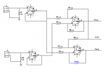
My first thought is a pair of buffers driving a pair of differential amplifiers referenced to the right voltage for the ADC. The input buffers may need to be mixed (discrete+opamp) circuits. The differential amps will require some precision resistors and it may be possible to add the active common mode rejection. Its sketched in the image below. I have not tested it and this is not fully "baked" yet. The opamps shown are placeholders. it only needs 8 precision resistors. The opamps however need to be able to drive 1K (600 Ohms?) without distortion and it still may limit the dynamic range. Depending on the input requirements it can be scaled to have gain or loss to some extent.
Its just a starting point. The input buffer opamps need to be exceptionally good to meet the requirements above.
I have been thinking about the analog interface problem since you sent the PM to me. Let me outline the issues so the magnitude of the problem is clear-
1) Signal to noise ratio needs to be greater than an AK5394A in all expected modes, that means 123 dB or more. (the detailed definition of this is more complex)
2) Distortion products must all be less that -115 dB
3) High common mode rejection differential input, so you get only the signal you want.
4) differential out symmetrical around the midpoint
5) High input impedance so it doesn't affect the source
6) Input induced nonlinearity needs to be very low so it doesn't add distortion to high impedance sources
The signal to noise requirements dictate high voltages and low impedances. The max P_P voltage on the input is 2.4V for each input or 4.8V P-P (1.7V RMS) differentially for FS out. The noise needs to be-124 or more dB below this. The distortion should also be less than this if possible.
AKM uses a simple 3 opamp solution that relies on either a good differential source or using an opamp to make a single ended source into a differential out (inverter). While this works it does not have much common mode rejection and requires active intervention to go from differential to single ended.
Circuits like the THAT differential design are low impedance input and require very close matched resistors (On the chip in the THAT and similar differential parts). However the resistor value may still limit the noise floor and will affect some sources.
My first thought is a pair of buffers driving a pair of differential amplifiers referenced to the right voltage for the ADC. The input buffers may need to be mixed (discrete+opamp) circuits. The differential amps will require some precision resistors and it may be possible to add the active common mode rejection. Its sketched in the image below. I have not tested it and this is not fully "baked" yet. The opamps shown are placeholders. it only needs 8 precision resistors. The opamps however need to be able to drive 1K (600 Ohms?) without distortion and it still may limit the dynamic range. Depending on the input requirements it can be scaled to have gain or loss to some extent.
Its just a starting point. The input buffer opamps need to be exceptionally good to meet the requirements above.
Attachments
@ Demian,
Thanks for your elaborate feedback and encouragement.
1) I agree. If we want a total SNR of 122 dB the front end SNR must be at 129 dB. If we want 122.5 dB the front end must be at 132 dB.
2) I agree. Again the target is to get the front end distortion well below the distortion of the ADC, to avoid degrading the total too much.
3) As I tried to explain in the initial post, I plan to split the design into an input part (on one PCB) and an ADC buffer part (on another PCB, together with the ADC). So, referring to your schematic the two op-amps on the left would be the input part and the two op-amps on the right would be the ADC buffer part. Depending on how the input part is made, the buffer part may also have to show a good common mode rejection. With the simple design in your schematic the ADC buffer part would have to provide all the common mode rejection.
4) Yes.
5) Yes.
6) Yes.
Comment to 3): For the input part I may try out different designs. This could include:
A) Simple op-amp based, similar to what you have shown on the schematic. Many op-amps seem to have problems with common mode distortion though (Samuel Groener http://www.sg-acoustics.ch/analogue_audio/ic_opamps/pdf/opamp_distortion.pdf). Maybe an AD797 could achieve a decent performance here. I have a suspicion that the common mode distortion is responsible for the relatively poor THD+N performance (at high levels) of figure 10 in the AK5394A data sheet.
B) An input stage, using the LSK389, to achieve a very low noise performance at all input impedance levels, could also be interesting to design and test. It could be an interesting way to achieve the goal of 5) above. Hopefully it will also address 6) above.
Of course the input stage should also include gain and attenuation to give some flexibility in terms of being able to measure very low noise levels as well as relatively high voltage levels. I might sacrifice e.g. a 150V input option and stay with a maximum of e.g. 15Vrms to keep the design simpler. In case I want to measure power amplifier performance I could add an external attenuator.
At the moment I try to concentrate on the ADC buffer part. Therefore a relatively low input impedance is not a big problem, as long as it is possible to drive it with normal op-amps with good noise and distortion performance and does not require special op-amps with a high current drive capability, but perhaps lower noise and distortion performance.
@ electroj,
Thanks for the reference. No, I had not seen that paper before.
Thanks for your elaborate feedback and encouragement.
1) Signal to noise ratio needs to be greater than an AK5394A in all expected modes, that means 123 dB or more. (the detailed definition of this is more complex)
2) Distortion products must all be less that -115 dB
3) High common mode rejection differential input, so you get only the signal you want.
4) differential out symmetrical around the midpoint
5) High input impedance so it doesn't affect the source
6) Input induced nonlinearity needs to be very low so it doesn't add distortion to high impedance sources
1) I agree. If we want a total SNR of 122 dB the front end SNR must be at 129 dB. If we want 122.5 dB the front end must be at 132 dB.
2) I agree. Again the target is to get the front end distortion well below the distortion of the ADC, to avoid degrading the total too much.
3) As I tried to explain in the initial post, I plan to split the design into an input part (on one PCB) and an ADC buffer part (on another PCB, together with the ADC). So, referring to your schematic the two op-amps on the left would be the input part and the two op-amps on the right would be the ADC buffer part. Depending on how the input part is made, the buffer part may also have to show a good common mode rejection. With the simple design in your schematic the ADC buffer part would have to provide all the common mode rejection.
4) Yes.
5) Yes.
6) Yes.
Comment to 3): For the input part I may try out different designs. This could include:
A) Simple op-amp based, similar to what you have shown on the schematic. Many op-amps seem to have problems with common mode distortion though (Samuel Groener http://www.sg-acoustics.ch/analogue_audio/ic_opamps/pdf/opamp_distortion.pdf). Maybe an AD797 could achieve a decent performance here. I have a suspicion that the common mode distortion is responsible for the relatively poor THD+N performance (at high levels) of figure 10 in the AK5394A data sheet.
B) An input stage, using the LSK389, to achieve a very low noise performance at all input impedance levels, could also be interesting to design and test. It could be an interesting way to achieve the goal of 5) above. Hopefully it will also address 6) above.
Of course the input stage should also include gain and attenuation to give some flexibility in terms of being able to measure very low noise levels as well as relatively high voltage levels. I might sacrifice e.g. a 150V input option and stay with a maximum of e.g. 15Vrms to keep the design simpler. In case I want to measure power amplifier performance I could add an external attenuator.
At the moment I try to concentrate on the ADC buffer part. Therefore a relatively low input impedance is not a big problem, as long as it is possible to drive it with normal op-amps with good noise and distortion performance and does not require special op-amps with a high current drive capability, but perhaps lower noise and distortion performance.
@ electroj,
Thanks for the reference. No, I had not seen that paper before.
Here are a few implementations that didn't copy AKM's or Crystal's schematics from the data sheets. First one is for A/D's with dual +/-5V supply, the other two - for the A/D's with single +5V. Perhaps they'll give you some ideas..
Best,
Best,
Attachments
That reference is very interesting. I think experimentation is necessary before any commitment to a design can be done.
Today's notes-
On my board one channel has the stock 5534's and I swapped the other channel for LME49710's. The LME channel has consistently 10-20 dB lower distortion with -115 to -125 dB harmonics. I tried an AD797 but it was not happy. Same for an LT1115. I did not dig deep. The circuit is documented on the datasheet. Its pretty simple but doesn't address some of the issues outlined above. It is interesting to note that the demo board has a resistor isolation in the output that the datasheet skipped. Also that it doesn't buffer the Vref. The datasheet notes that a small offset will reduce the zero signal noise. All something to explore.
I don't think casually separating the input buffers from the differential circuitry is a good idea since they will work closely. They do need to be part of the same design effort. However a differential attenuation solution should not be difficult. Extra gain may be useless if the input noise floor is scaled correctly at around 1 nV/rtHz (if possible, less that 5 nV/rthz is a reasonable goal that would not limit much.) I have some FET buffered opamp "impedance converters" I'm toying with. The best circuit I know of, the input amp for the Shibasoku 725, is not that hard to build or that expensive. It does use a number of discretes, 15 transistors including a pair of Jfets and it does get down to -130 dB THD. However I do think its possible to get to the same place with a hybrid of discretes and opamps.
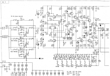
Here are a few notes from my efforts today at getting the AKD5394A demo board running. it was a bigger effort that I had expected since I did have it running before.
First a few notes on settings (for me as well as anyone else). The datasheet settings woork for 48KHz. To get the unit running at 192KHz- Dip switches: SW2 #1 on, SW3 #6 on. Jumpers- JP7 CLK, JP9 12.288, JP11 12.288, JP12 192K, JP13 74HC74. The digital and analog parts do not share a ground so you need to provide one if your supplies are isolated.
The on board crystal oscillator has a lot of spurs that show up in the output. You need to use a clean external oscillator for best results.
Today's notes-
On my board one channel has the stock 5534's and I swapped the other channel for LME49710's. The LME channel has consistently 10-20 dB lower distortion with -115 to -125 dB harmonics. I tried an AD797 but it was not happy. Same for an LT1115. I did not dig deep. The circuit is documented on the datasheet. Its pretty simple but doesn't address some of the issues outlined above. It is interesting to note that the demo board has a resistor isolation in the output that the datasheet skipped. Also that it doesn't buffer the Vref. The datasheet notes that a small offset will reduce the zero signal noise. All something to explore.
I don't think casually separating the input buffers from the differential circuitry is a good idea since they will work closely. They do need to be part of the same design effort. However a differential attenuation solution should not be difficult. Extra gain may be useless if the input noise floor is scaled correctly at around 1 nV/rtHz (if possible, less that 5 nV/rthz is a reasonable goal that would not limit much.) I have some FET buffered opamp "impedance converters" I'm toying with. The best circuit I know of, the input amp for the Shibasoku 725, is not that hard to build or that expensive. It does use a number of discretes, 15 transistors including a pair of Jfets and it does get down to -130 dB THD. However I do think its possible to get to the same place with a hybrid of discretes and opamps.
Here are a few notes from my efforts today at getting the AKD5394A demo board running. it was a bigger effort that I had expected since I did have it running before.
First a few notes on settings (for me as well as anyone else). The datasheet settings woork for 48KHz. To get the unit running at 192KHz- Dip switches: SW2 #1 on, SW3 #6 on. Jumpers- JP7 CLK, JP9 12.288, JP11 12.288, JP12 192K, JP13 74HC74. The digital and analog parts do not share a ground so you need to provide one if your supplies are isolated.
The on board crystal oscillator has a lot of spurs that show up in the output. You need to use a clean external oscillator for best results.
I have also seen very good performance with the LME49710. I used 2x LME49710 in a 1kHz low distortion oscillator. As far as I could measure, using a notch filter and an ADC, the THD was at -151 dB with an output level of around 2.8Vrms. In that design both op-amps are used in the inverting mode. But I could imagine that the distortion in the non-inverting mode is also a lot lower than the distortion of the 5534.
I think that with the circuit AKM is usung, it doesn't need to buffer the reference, since it goes straight into the non-inverting input of the op-amps. Obviously with your differential circuit above, a buffer is needed.
The trick with the DC offset I have actually used many years ago on a telecom codec, where the ADC needed it to remove an annoying tone in the audio band. Applying a DC moved the tone outside the audio band.
I hope to get down to around 2nV/rtHz, but it is not easy to get there and may turn out to be impossible, when other design goals also have to be met. A design with JFET inputs and a distortion around -130 dB sounds like some of the right stuff.
I don't have an AK5394A demo board, but I could imagine that the crystal oscillator, based on a CMOS inverter, is not the optimum solution. And other inverters in the same IC is even used for other signals.
Shibasoku 725 input amp
Here is one effort. The cascoded JFETS on the input have very low input capacitance and it doesn't change in operation. However the noise is limited since the JFET noise is in series with the bipolars. in practice this circuit is about 5 nV/rtHz. Its possible to get lower if the JFETS are the input without the bipolar parts but other issues getting stability etc come crawling out of the woodwork.
It may be possible to tie the cascoded JFETS to the offest pins of the right type of opamp (LT1115). Seems like a lot of hassle for a small return but that's what a lot of this is about.
Attachments
It looks like R2 in the input circuit alone contributes around 5nV/rtHz. And then there is a similar contribution from the feedback network. Reducing R2 should allow a lower noise level, but of course it makes it easier to damage the input FET.
I have done some simulations on a design with the LSK389 + a cascode, followed by an op-amp. It has a differential input and single output. I will try to make a cleaned up schematic and post it. It may take a few days to get it done.
But I have not tested it.
I have done some simulations on a design with the LSK389 + a cascode, followed by an op-amp. It has a differential input and single output. I will try to make a cleaned up schematic and post it. It may take a few days to get it done.
But I have not tested it.
You are right about R2. Notice its a 7W resistor. It would need to handle a fair amount of fault current it seems. Maybe a fuse would be an interesting alternative.
Below is a take on the same cascoded idea. The mosfets are depletion mode which really simplifies the circuit. Adding it as a first stage with gain is more difficult to make stable. As it is the response is flat with as high as 50K source Z. Needs to be built to confirm it really can work this way. The LT1010 is not necessary.
Below is a take on the same cascoded idea. The mosfets are depletion mode which really simplifies the circuit. Adding it as a first stage with gain is more difficult to make stable. As it is the response is flat with as high as 50K source Z. Needs to be built to confirm it really can work this way. The LT1010 is not necessary.
Attachments
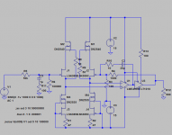
I have made a schematic, which shows what I am thinking of for the input stage. It is based on a design from the Stanford Research SR770, modified with a FET cascode, protection diodes on the input, some updated component choices and other changes.
Compared to the schematic shown in the previous post, I have moved the op-amp to the drain side of the input pair, so I get some gain here, improving the noise level. I know that it will be a challenge to keep it stable. But at least it would be worth trying.
I have simulated it in TINA TI with good results for noise and distortion. But I am not sure how much I can rely on this simulation, especially regarding the distortion. So of course I will need to test it in a real design.
Any comments to the design? Are the cascode FET's a good choice? Should they be paired? I don't have much experience in FET design. I have used the 2SK389 in a headphone amplifier I built some time ago, but it didn't have a FET cascode. For this design I chose the LSK389 instead due to availability and noise performance.
The resistor tolerances may not be correct in this schematic.
Actually I started with the ADC buffer stage and now suddenly we are looking at the input stage 😛
Attachments
You are right about R2. Notice its a 7W resistor. It would need to handle a fair amount of fault current it seems. Maybe a fuse would be an interesting alternative.
Below is a take on the same cascoded idea. The mosfets are depletion mode which really simplifies the circuit. Adding it as a first stage with gain is more difficult to make stable. As it is the response is flat with as high as 50K source Z. Needs to be built to confirm it really can work this way. The LT1010 is not necessary.
Demian can you post the non generic LT models for this circuit?
Here is some of the models. I have no experience with Tina so i don't know how to "port" the models but they are all pretty generic. The Supertex models came from Supertex. Your circuit looks ok. I used depletion mode mosfets from Supertex for the cascode which work well. The source resistors you are using see high. It gives a wider stability margin but higher noise and lower gain on the first stage. All tradeoffs to be managed.
Distortion measurements in Spice are not worth much once the circuit is linear.
I need to find time to breadboard some of these circuits.
Distortion measurements in Spice are not worth much once the circuit is linear.
I need to find time to breadboard some of these circuits.
Attachments
I have studied the Amber 3500 input before. Its pretty trick, replacing the input bipolars with the Jfets. Cascoded this way the input cap drops a lot. Cascoding with bipolar transistors brings a lot of parts to do it.
The other interesting trick is the lighbulbs and the transistors connected at diodes for input protection.
The other interesting trick is the lighbulbs and the transistors connected at diodes for input protection.
I once made some simulations of different cascode circuits with JFET's and bipolars. At least in the simulation I got better performance with the JFET-based circuits. And of course the bipolar variants need a lot of components.
My main worry with the JFET-based version is the spread on the Vgs.
My main worry with the JFET-based version is the spread on the Vgs.
Usually you can get 5 mV between devices in duals. That can be dialed out with a trimmer and the remaining temp/voltage and time drift is pretty small. I have been using this type of circuit on products for many years with no issues. If absolute DC accuracy is required then a separate chopper circuit could be added.
Usually you can get 5 mV between devices in duals. That can be dialed out with a trimmer and the remaining temp/voltage and time drift is pretty small. I have been using this type of circuit on products for many years with no issues. If absolute DC accuracy is required then a separate chopper circuit could be added.
I think what he meant was, does the cascode JFET's have to be paired?
- Status
- Not open for further replies.
- Home
- Design & Build
- Equipment & Tools
- Buffers for ADC design with AK5394A and other ADC's ?