Actually I prefer the 550/560 instead of the 546/556 types. Not only they have a slightly higher Vce0, and perhaps even gain, but they are also even lower noise.
Plus those are plentiful available. You can find them from multiple sources, like mouser, and several manufacturers make them (on semi / fairchild, nxp...)
I got some of those fairly recently. Stocking up large enough batches to match some pairs/sets. With enough of them, it's more likely that making closer sets will be easier.
Not always easy to match the NPNs to the PNPs in sets, but I surely will try hard on that.
Eh? The BC550 has a Vceo of 45V and the BC546 has a Vceo of 65V. Given that the supply voltage is +/-33V using the BC550/560 for vas duty would be a bit of a stretch.
We may be talking at cross purposes. I recommend the BC546/556 for vas only and the BC550/560 for the input differential pairs as you suggested.
Sorry, you're right about the Vce0, but there is nothing to worry about with the +/-33V supply, as each "side" only sees about one of those supplies anyways.
I ran a lot of sims and checked on that aspect, and to come even close to the limits, you'd have to saturate that stage to clipping, and even then, it's still not exposing each side to the full voltage swing. So I wouldn't worry about it and use those lower noise parts.
The 549/559 parts really have overly low Vce0, so I don't bother with those, but the 550/560 are quite suitable.
We may be talking at cross purposes. I recommend the BC546/556 for vas only and the BC550/560 for the input differential pairs as you suggested.
Yes, the diff pairs only. And we can even go a bit higher in rails voltage, since we never ever come close to clipping those stages anyways. That keeps them well within operating range and lowers distortion.
Just to clarify - we're talking about the input stage discrete opamps here. For the power amp section the PN100/200A diff pairs can be replaced with the BC550/560,as before, but the 2N5401/5551 vas is fine as is, and the parts are still available.
The PN100/200 parts also have their Vce0 at 45V, so same as the BC550/560 ones, and since the power amps input stages are also powered with their rails at 33V, just like those discrete opamps, then the BC550/560 can be used there as well, even for the VAS stages, since that too is on the same 33V rails. Bryston use those PN100/200 there for the VAS stages, in the power amps, so there is nothing preventing the use of the BC550/560 instead. And the gain is much better on those BCs compared to those PNs...
I hear what you say and its a reasonable position. However at full output the vas transistors are going to see a Vce of about 60V, albeit for short periods of time. So I prefer to use vas transistors with a Vceo greater than the total supply voltage ( 66V ). I may be a bit overcautious as the measured Vceo of most transistors is usually quite a bit higher than the datasheet value. However I always try to cater for the very worst case and make my designs bullet proof. I wonder how well the PN100A/200A vas would cope with a 20Hz square wave at full output with +/-33V supplies. I mentioned the 2N5401/5551 because thats what Bryston use for the vas in the power amp section.
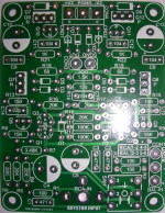
I got one of the small Bryston input boards shown below to check out my proposed substitutions modifications. These are:-
Q1 BC550C Q7 KSC2690AY
Q2 BC560C Q8 KSA1220AY
Q3 BC550C Q9 MJE182
Q4 BC560C Q10 2N5551
Q5 BC546C Q11 2N5401
Q6 BC556C Q12 MJE172
R8, R9 6.2k R11, R12 68k or E-501 0.5mA CRD
R18, R19 43R
C4, C5 100u 35V Non Polar
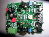
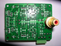
And a couple of photos of the finished pcb are also shown below. With these modifications the VAS standing current is reduced from approximately 12mA to 6mA whilst the quiescent current of the output devices remains at around 13mA. Note that the KSC2690AY/KSA1220AY devices have roughly double the gain of the devices originally specified. If you don't have any BC550C/BC560C then the KSC1845/KSA992 pair can be used with a bit of lead dressing. The BC546C/BC556C pair are still in production at Diotec Semiconductor.
Q1 BC550C Q7 KSC2690AY
Q2 BC560C Q8 KSA1220AY
Q3 BC550C Q9 MJE182
Q4 BC560C Q10 2N5551
Q5 BC546C Q11 2N5401
Q6 BC556C Q12 MJE172
R8, R9 6.2k R11, R12 68k or E-501 0.5mA CRD
R18, R19 43R
C4, C5 100u 35V Non Polar
And a couple of photos of the finished pcb are also shown below. With these modifications the VAS standing current is reduced from approximately 12mA to 6mA whilst the quiescent current of the output devices remains at around 13mA. Note that the KSC2690AY/KSA1220AY devices have roughly double the gain of the devices originally specified. If you don't have any BC550C/BC560C then the KSC1845/KSA992 pair can be used with a bit of lead dressing. The BC546C/BC556C pair are still in production at Diotec Semiconductor.
Attachments
The schematics of both of the Bryston input boards are the same. I don't want to post the original schematics here in case I fall foul of copyright, but I am going to redraw the schematics incorporating my modifications and will post them here. Q7/Q8 are the output devices. Q9/Q12 are the regulator devices and I left them as is because the type is not important for this function.
A few notes about my implementation. All of my BC type transistors have an hfe of close to 550 and the KSA/KSC pair have an hfe of close to 250. As a result of this excellent matching the output offset is only 700uV. A 10kHz square wave is clean with fast edges and no sign of under/over-shoot. The VAS devices Q5/Q6 now run much cooler as they are only dissipating 200mW as opposed to 400mW originally.
A few notes about my implementation. All of my BC type transistors have an hfe of close to 550 and the KSA/KSC pair have an hfe of close to 250. As a result of this excellent matching the output offset is only 700uV. A 10kHz square wave is clean with fast edges and no sign of under/over-shoot. The VAS devices Q5/Q6 now run much cooler as they are only dissipating 200mW as opposed to 400mW originally.
regarding your pics
R8 and R9 are different from 15k
R11 and R12 are diodes
R18 and R19 are not 68 ohms
I have same input board but no MJ trans, so Q7,Q8 will be BD139/140
and TIP122/127 for Q9-Q12
R8 and R9 are different from 15k
R11 and R12 are diodes
R18 and R19 are not 68 ohms
I have same input board but no MJ trans, so Q7,Q8 will be BD139/140
and TIP122/127 for Q9-Q12
bobina if you look back to post #369 you'll see I detail all of the changes I made to the parts you mentioned. I made the changes because the PN100A/PN200A are obsolete. I know, so are the BC560C but I have a large stash of them, as do many other people. If you want current production devices then use the KSC1845/KSA992 pair ( with a bit of lead dressing ). I changed the resistor values so that the quiescent current of the VAS transistors Q5/Q6 was cut from 12mA to 6mA. At the original current Q5/Q6 were dissipating 400mW and ran pretty hot - now they run cool. To cut the loading on Q5/Q6 now that the standing current was reduced I used output devices with potentially 4x the hfe of the MJE172/MJE182. I've redrawn the schematic with my revised parts values and attached it to this post.
Attachments
No the pictures and the schematic are the same. I used 0.5mA constant current diodes instead of resistors for R11,12. If you use resistors for R11,12 I changed the recommended value from 68k to 62k
Sorry, you're right the pictures show the penultimate version when I was still experimenting. The schematic is the final version.
I've run the input board from +/-42V supplies and you might be able to go down to +/-40V, but I wouldn't go any lower. As regards the maximum supply voltage you're limited by the dissipation in Q9, Q12. If you're using the originally specified components I'd say +/-70V would be the maximum. If you're using my modified version of the input board, which draws less current overall, then you might be able to push it up to +/-85V. In both cases that assumes that you're using heatsinks on Q9, Q12 as shown in my pictures. If you reduce the value of the zener diodes VD1, VD2 then you can use even lower supply voltages ( at the expense of dynamic range ). I'd say VD1=VD2=15V with a supply of +/-24V represents the absolute minimum.
Thank you for the fast answer. I wanted to use the input board for another power amplifier. There I only have +/- 35V available.
- Home
- Amplifiers
- Solid State
- Bryston 4B SST clone