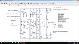
Aren't the right side Q1 and Q3, together with the base diodes, actually current mirrors? If the BE junctions ratio is 1 then the diodes and Q1/Q3 currents are equal and the delta between the base and the collector current sources forward biases the output pair through the 2 diodes in series. Is this some sort of sliding bias scheme?
I'll look at it some more but first take is an absolutely minimal CFA used backwards. It seems to do the right thing but I have to explore its warts. Listening to some old Cockney Rejects BTW.
@Bob
Have you ever seen this used anywhere? On the far left is Barry Blesser's "super" transistor IMO a different take on the CFP, published in 1968 IIRC. I took it in progression to the far right, something that behaves a lot like the two CFP output stage kind of an error corrected (with feedback) buffer. You synthesize a high input impedance from what is inherently a low one rather than a low output impedance from what is inherently a high one, an interesting flip-flop. The designer has a lot more control of the drive end than the load that gets hanged on the output, food for thought.
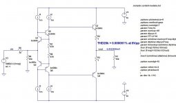
For some time I am trying to design simple inverting buffer but not satisfactory up to now.
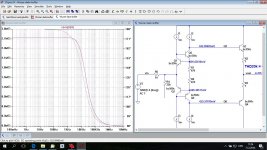
During that process, I came to this non inverting buffer with no global NFB and very low distortion.
It has almost the same distortion as the one from the last Wurcer schematic.
BR Damir
Attachments
Last edited:
For some time I am trying to design simple inverting buffer but not satisfactory up to now.
During that process, I came to this non inverting buffer with no global NFB and very low distortion.
It has almost the same distortion as the one from the last Wurcer schematic.
BR Damir
What sets the potential between the bases of Q3/Q4?
Finally we have the opportunity to ask ourselves: why does the world's lowest noise device (AD797) use current source loads on the input stage, rather than resistor loads? Are resistor loads STUPID?
Feel free to answer that for yourself. Replacing Q1 with a resistor that supports 90mA
bias current requires excessive Vcc or the gain of the first stage falls through the ground
and it takes the noise performance with it.
The expression "active loads tend to amplify their own noise" is a verbatim citation
from Gray&Meyer and that's one of the very few points where G&M stay vague.
regards, Gerhard
Attachments
Last edited:
Feel free to answer that for yourself. Replacing Q1 with a resistor that supports 90mA
bias current requires excessive Vcc or the gain of the first stage falls through the ground.
I think I already answered his question, the 797 actually used resistors to Vcc with pnp's in folded cascode. Active loads frequently eat headroom. The real fun is mixing bi-polar and FET's the gm mismatch gives plenty of opportunities for unwanted noise gain. Some of the bandaids in the 743 are embarrassing. I was also told by the CEO/CTO of a major sonar company that these effects don't exist because he never saw them. So no surprise it keeps turning up.
What sets the potential between the bases of Q3/Q4?
R7, R8, off course this in not working schematic just just my stumbling on it when tried to make inverting buffer, that why there two resistor, FB input.
Scott maybe you have some ideas how to make simple low distortion inverting buffer, with or without NFB?
I designed one but to complicate for my taste.
thanks, Damir
For some time I am trying to design simple inverting buffer but not satisfactory up to now.
During that process, I came to this non inverting buffer with no global NFB and very low distortion.
It has almost the same distortion as the one from the last Wurcer schematic.
BR Damir
Seems the current in OPS is very high...... too high for those devices??
I tried also to make ULD buffer but also ended up with it being too many transistors.
THx-RNMarsh
Last edited:
Seems the current in OPS is very high...... too high for those devices??
I tried also to make ULD buffer but also ended up with it being too many transistors.
THx-RNMarsh
Richard, OPS bias current for that simulation was 1.6 mA only.
Actually I would like to have quite low power consumption and low distortion in the same time.
BR Damir
R7, R8,
How so? Humor me for a second. In the quiescent state you have two Vbe's across 470+470 Ohms which for any silicon transistor I have ever seen is >1mA, but the loop is trying to force Q5 and Q6 to be at 1mA collector current so the loop can not be satisfied and the collector voltages of Q5 and Q6 are undefined (actually they saturate).
How so? Humor me for a second. In the quiescent state you have two Vbe's across 470+470 Ohms which for any silicon transistor I have ever seen is >1mA, but the loop is trying to force Q5 and Q6 to be at 1mA collector current so the loop can not be satisfied and the collector voltages of Q5 and Q6 are undefined (actually they saturate).
Yes and thus force the Vb of Q3/Q4 very low - to the voltage across R7, R8 and thus lead to low current in Q3/Q4.
Jan
How so? Humor me for a second. In the quiescent state you have two Vbe's across 470+470 Ohms which for any silicon transistor I have ever seen is >1mA, but the loop is trying to force Q5 and Q6 to be at 1mA collector current so the loop can not be satisfied and the collector voltages of Q5 and Q6 are undefined (actually they saturate).
Yes you are right, the collector voltages Q5 and Q6 are very low.
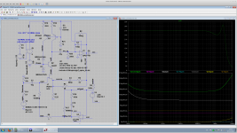
Attached simulation with the collector voltages under signal swing. It could be that simulator gives wrong result in this case?
Attachments
Yes you are right, the collector voltages Q5 and Q6 are very low.
Attached simulation with the collector voltages under signal swing. It could be that simulator gives wrong result in this case?
You probably end up driving the output directly with the input source some how with very little to distort.
You probably end up driving the output directly with the input source some how with very little to distort.
Yes, but with high input impedance and output easy to drive 10k, in other words, buffer.
Only problem for me it does not invert.
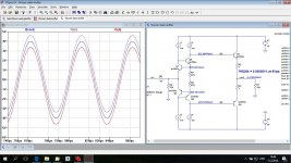
Repeat the sim with R6 = 1k and see what happens.
Input impedance is quite high.
Attachments
Sorry for intruding on such detailed topics, but again, as a novice question, do fully balanced designs not deserve more book space than a mere 3 pages?
Hi SGK,
I can't see why. There isn't anything too different and the circuits are the same, just doubled. Differential input and outputs to convert between single ended and balanced are the only thing different, and they are dealt with in any discussion about microphones or professional sound equipment.
Balanced signal paths are only beneficial when they solve a problem. If there isn't a problem, like excessive radiated noise being picked up in the connecting cables, you are often better off using a standard, single ended plan. Going balanced will cause a 1.414 times noise increase. The overall noise will depend on levels in case you are doubling the signal amplitude.
-Chris
Hi Chris
Unless of course your source only has balanced outputs (such as mine).
I'm not talking about a single-ended typology which requires an input board to convert a balanced input to a single-ended one. I have done that and built Self's ultra low noise balanced to single-ended circuit. (I continue to battle noise in the overall amp.) And I am not talking about bridged amplifiers, but rather "true balanced amplifiers [which] comprise a single amplifier whose circuitry is balanced from input to output" to quote Bob pg 533.
I was admiring the SAE 8300 8 channel amp from SAE, part of Morris Kessler's stable. (Amazingly, to me at least, each channel's PSU and amp are all on one (stackable) PCB and yet it achieves commendable SNR.)
Hi SGK,
I've worked on both types of gear a lot. For the home especially, balanced doesn't buy you a lot. It does cost a lot though. You're doubling the circuitry. If you are running long distances, or have an RFI problem, then balanced might help you solve those issues, but you pay a price. If those issues don't exist, then you really were better off with a single ended version.
The best balanced device will be bested by an identical single ended version. The Carver Direct is an example of a balanced through-out preamplifier. Doesn't buy you much.
As for your source, it is single ended internally with the balanced adapter hanging off the output. If they ran it balanced right from the DAC out, it just simply added cost to the unit.
Best, Chris
- Home
- Amplifiers
- Solid State
- Bob Cordell's Power amplifier book