Edmond Stuart said:Hey Bob, where are you? Running out of text or still puzzled by that patent?
Hi Edmond,
Neither.
Do you miss me? 🙂.
Actually, I have been unbelievably busy at work the last couple weeks. I have spent what little time I have had over on the Blowtorch thread trying to contribute some constructive input on PIM.
I have not looked at the patent, but I did look at the figure you posted a few posts back. I agree that taking Miller compensation from the VAS collector node or from the following emitter follower in that particular circuit will likely disrupt the EC function.
Cheers,
Bob
Hi🙂
I have a question regarding Bob's hexfet output stage configuration and thermal biasing. If a single BJT can compensate both hexfets, I don't see why adding a separate Vbe multiplier like this wouldn't work. Of course, that doesn’t mean it will work. Maybe it's been discussed before but I missed it. My goal is to push the bandwidth of the EC amplifier by using small signal SMD's and minimizing trace lengths. Is this a prudent direction to take?
(compensation not included)
I have a question regarding Bob's hexfet output stage configuration and thermal biasing. If a single BJT can compensate both hexfets, I don't see why adding a separate Vbe multiplier like this wouldn't work. Of course, that doesn’t mean it will work.
Maybe it's been discussed before but I missed it. My goal is to push the bandwidth of the EC amplifier by using small signal SMD's and minimizing trace lengths. Is this a prudent direction to take? (compensation not included)
Attachments
CBS240 said:Hi🙂
I have a question regarding Bob's hexfet output stage configuration and thermal biasing. If a single BJT can compensate both hexfets, I don't see why adding a separate Vbe multiplier like this wouldn't work. Of course, that doesn’t mean it will work.
(compensation not included)
Hi CBS240,
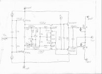
It is a worthy goal to get the EC differential amplifier off of the heat sink and close in to the rest of its related circuitry. That was a compromise that I took in my original MOSFET EC amplifier, namely placing one of the EC differencing amplifier transistors on the heatsink to acheieve the needed temperature compensation.
I have since toyed with various ideas on how best to leave the differencing amplifier transistor off of the heatsink and achieve the necessary temperature compensation by other means, but have not seriously pursued any of those.
Cheers,
Bob
I decided to spend some otherwise idle time burning up a few brain cells on ways to eliminate the need for heat sinking the error difference amplifier transistors. IMHO this is one of those experiments that may be better to build a real circuit instead of relying on just calc and sim......
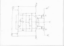
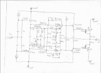
This is a quick sketch of a circuit option that seems to work correctly, for the most part🙄. I measure a difference between points A and Vout that is consistent with what I expect to see driving the changing Vgs WRT Iout. Q: Is there any significant drawbacks for using J-fet’s for the EC difference amplifiers? If the whole amplifier DC offset is controlled by a servo, a small difference in Vgs for the P and N channel J-fet’s @ Id shouldn’t be to big of an issue as long as they are close. The J-fets' bias is around the 0 tempco Qp. I like the self-bias characteristic for this part of the circuit. If one is OK with sacrificing a few more volts, then I suppose adding a single Vbe multiplier isn’t out of the question. That part of the circuit works good giving an overall slightly negative tempco. I measured DC voltage levels with 150mA outputs’ bias using 0.1 Ohm source resistors.

This is a quick sketch of a circuit option that seems to work correctly, for the most part🙄. I measure a difference between points A and Vout that is consistent with what I expect to see driving the changing Vgs WRT Iout. Q: Is there any significant drawbacks for using J-fet’s for the EC difference amplifiers? If the whole amplifier DC offset is controlled by a servo, a small difference in Vgs for the P and N channel J-fet’s @ Id shouldn’t be to big of an issue as long as they are close. The J-fets' bias is around the 0 tempco Qp. I like the self-bias characteristic for this part of the circuit. If one is OK with sacrificing a few more volts
, then I suppose adding a single Vbe multiplier isn’t out of the question. That part of the circuit works good giving an overall slightly negative tempco. I measured DC voltage levels with 150mA outputs’ bias using 0.1 Ohm source resistors. Attachments

Hi
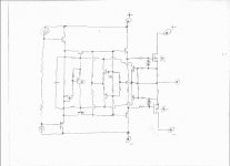
Burned up a few more brain cells and reconfigured the circuit to this. The results are a bit better. There was a small instability with the J-fet circuit. It was very touchy and had the tendency to lock up and start oscillating.
The P-ch J-fet's Vgs are matched at Id; Vgs=2V. I happen to have more P-ch J-fets in the drawer than N-ch.🙂 The difference amplifier transistors bias is about 1mA. The Vbe multiplier bias is 2.6mA and still seems to create a slight overall negative tempco. I will play with this circuit some more and try to tweak it a bit better. Any tips as to what details I should concentrate on?😕
Attachments
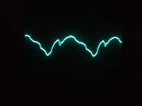
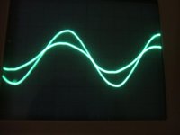
CBS240 said:Here is the difference voltage measured at point A and Vout.
f=100KHz
Vout=10Vp
load is 5 Ohms resistive.
I think that sharp "V" shape in the curve may be a crossover related distortion component.
Would you have this picture with the input signal in it as reference?
Jan Didden
OK
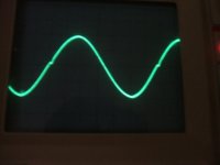
I figured out the problem...To limit any possible smoke signals, I was using a 15VA transformer to test the DC bias. It wasn't quite up to driving 10Vp into 5 Ohms. Replacing the power transfo with a larger one, the error signal looks more rounded.
This is the error difference with 10Vp @ 150KHz driving 5 Ohms.
I figured out the problem...To limit any possible smoke signals, I was using a 15VA transformer to test the DC bias.
It wasn't quite up to driving 10Vp into 5 Ohms. Replacing the power transfo with a larger one, the error signal looks more rounded. This is the error difference with 10Vp @ 150KHz driving 5 Ohms.
Attachments

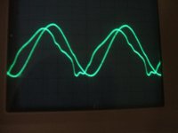
This is the output signal.
I'm having problems getting rid of that small crossover component on the positive swing.😡 Some more tweaking is needed. It seems the differencing amplifiers are quite sensitive to ambient temperature. Wouldn't reducing thier gain decrease the influence of thier tempco effects?
I'm having problems getting rid of that small crossover component on the positive swing.😡 Some more tweaking is needed. It seems the differencing amplifiers are quite sensitive to ambient temperature. Wouldn't reducing thier gain decrease the influence of thier tempco effects?
Attachments
This is the input and output. The smaller signal is the output. The last waveform is actually inverted so the crossover notch is on the negative slope. There isn't much phase shift between input and output with this circuit. I like the idea of using it outside the nfb loop, just as a follower. A wire with current gain.😛 Now if I can only get it tweak out......perhaps if I increase bias to 300-400mA .....................
..................... Attachments
Hi C.K,
If you could show the input (or output) signal and the error signal in the same picture, that woud give us some additional info from the phase relationship.
Jan Didden
If you could show the input (or output) signal and the error signal in the same picture, that woud give us some additional info from the phase relationship.
Jan Didden
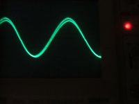
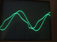
Hi Jan
OK, I see what you’re getting at. The problem is the function generator GND is referenced to the scope GND through the earth GND. I used a signal transformer to isolate the function generator and grounded the scope reference to the output. Then measured circuit GND with CH 2, inverted it, then measured point A with CH 1, non-inverted. The output sine wave is 5V/div, 10Vp, and the error signal is 1V/div, 1uS/div. This looks like an accurate representation of the phase difference at 150 KHz, w/200mA bias. Looks like a phase difference of about 800nS. It appears the error signal does try to "correct" that crossover glitch.
PS C. K. is the quoted, Charles Kettering
My name is Chris🙂
Attachments
CBS240 said:Hi Jan
OK, I see what you’re getting at. The problem is the function generator GND is referenced to the scope GND through the earth GND. I used a signal transformer to isolate the function generator and grounded the scope reference to the output. Then measured circuit GND with CH 2, inverted it, then measured point A with CH 1, non-inverted. The output sine wave is 5V/div, 10Vp, and the error signal is 1V/div, 1uS/div. This looks like an accurate representation of the phase difference at 150 KHz, w/200mA bias. Looks like a phase difference of about 800nS. It appears the error signal does try to "correct" that crossover glitch.
Yes. It seems to try to correct mainly 3rd harmonics, plus that glitch. Which could be a PNP turning on slow. At lower freq the 3rd harmonic would probably be more visible, without the glitch.
CBS240 said:[snip]PS C. K. is the quoted, Charles Kettering
My name is Chris🙂
My goof. Apologies, Chris.
Jan Didden
At lower freq the 3rd harmonic would probably be more visible, without the glitch.[/B]
Yes, it appears to not have the crossover glitch at a slower freqency, but the slope of the error voltage changes slightly around crossover so there must be some component of it still there, as I would expect. It's seems a bit worse on the negative slope though. The error signal does show what happens if you have no error correction circuitry and attempt to use hexfet's as class AB source followers. The distortions are obvious. Of course there is no NFB loop around this circuit, just straight in, straight out.
What I like is it can help to make the output less load dependent, since the load current depends on the ever changing speaker impeadance.

30KHz, 5uS/div.
Attachments
- Home
- Amplifiers
- Solid State
- Bob Cordell Interview: Error Correction