PB2 said:I was wondering if you looked at how the EC alters the input impedance of the output stage? The impedance seen from the output of Q4 and Q8 is what I had in mind.
I haven't looked at this with a sim of Bob's circuit. But the project files are contained in the .zip file I posted.
Hi,
is it low Vbe that hogs the base current (and collector current) and then allows the device to get hotter until destruction?
orjohn curl said:If you parallel output transistors, it is best to beta match them, because with an optimum Re (a low value R), the high beta ones will run away and blow up the amp. I have an amp in my lab (JC-1) that only worked after I personally hand matched the output devices (9 on each side).
is it low Vbe that hogs the base current (and collector current) and then allows the device to get hotter until destruction?
Andy-c
I agree with you that Mos with Cordell EC looks impressive.
I understand your comment on the distortion aspect. I believe that there are two aspects: relative amount of higher harmonics and level of harmonics. Don't you think that a wide Vin window of variation in the transfer characteristic ( Vout/Vin) will give high levels of harmonics ( signal is high when it meets non linearities) and a concentrated déformation will give as you said high frequency harmonics. Therefore optimum biasing is not straightforward to me in a theoretical way at least.
The reason why I asked the over biased run (IoRc = 52) is that I would like to make the transfer characteristic ( Rload/Rload + Rout) and then calculate a fourier transform of Vout and this for different settings.
I wonder if there is a burst of energy in the transistor followed by low level signal and if the thermal tracking has a delay, then Io will be very high and the system will be in a transient way fully overbiased for a while. This can be perhaps simulated with Spice.
Also I would like to investigate if the gain which is the derivative of Vout with respect to Vin cannot become positive for certain values of i out depending on goRc. A first look let me think that it is possible if Rcgo > 1.5. If this is true and if the thermal aspect can bring this situation, it could explain some bursts of oscillations and the creation of intermodulation products through feedback regeneration.
Perhaps I am totally wrong but it is fun
JPV
john curl said:If you parallel output transistors, it is best to beta match them, because with an optimum Re (a low value R), the high beta ones will run away and blow up the amp. I have an amp in my lab (JC-1) that only worked after I personally hand matched the output devices (9 on each side).
Mr Curl,
For low R, what level of beta maching is required to avoid these problems.
Thank you
JPV
Here’s a simplified schematic for an “error correction” scheme I’ve come up and have been experimenting with. The non-inverting input of the opamp (Vin) is essentially bootstrapped, so loading of the proceeding VAS is just about non-existent. THD performance blows Hawksford error correction out of the water.
Cheers,
Glen
Cheers,
Glen
john curl said:Actually, the table is very good.
Let me put some more info into this equation:
First, there is NO exact value for the resistor, but you will most probably have the best success with a 0 signal voltage drop of 15-26mV. This is the BEST FIT REGION for the transfer function.
However, you must drive the output transistors from a zero ohm source, to ideally match the equations. Since that is not practical, then Beta non-linearity and Rs/beta will also be part of the overall optimization of the transfer function.
For example, if you current drive the output transistors, then all bets are off. (equations too!)
This is a very good point, John. Driving the output transistor from a source that adequately approaches zero ohms is not easy, in light of finite beta of an output transistor. Actually, it occurs to me that your circuit, wherein you drive the output transistor with a MOSFET source follower, may be easier to analyze in this regard because it doesn't propogate the analysis all the way back to the VAS. It's driving impedance for the output transistor will be, I think, on the order of 1/its gm. If you bias the MOSFET driver at, say, 50 mA, its 1/gm will be on the order of 5 ohms. If the BJT has a beta of 50, then the impedance seen looking back into the emitter of the BJT is about 0.1 ohm, which is even still on the order of the RE. I think this makes your point, and adds a sobering consideration to interpreting Self's recommendation.
Bob
G.Kleinschmidt said:Here’s a simplified schematic for an “error correction” scheme I’ve come up and have been experimenting with. The non-inverting input of the opamp (Vin) is essentially bootstrapped, so loading of the proceeding VAS is just about non-existent. THD performance blows Hawksford error correction out of the water.
Cheers,
Glen
Hi Glen,
So, if I've got it right, this circuit is just a unity-gain voltage-follower op amp wherein its output is buffered inside the loop by the unity gain output stage. Am I correct? If this is the case, it just looks like pure NFB, but that's OK if it works.
Is it stable? What op amp do you have there? Are you bootstrapping the power supplies of the op amp or are you using an incredibly high-voltage op amp? By what measurement or analysis does it blow away HEC? Did you build it? Did you SPICE it? Did you measure full-power THD-20? THD-1 doesn't count - this circuit will obviously do very well at 1 kHz as long as you compensate it to be stable.
Thanks,
Bob
I think you will find the compensation requirement "interesting"
most spice op amp models will predict stable operation - and be WRONG
you need a multiple pole-zero macro-model that correctly references the gain stage to the power supply terminals
you have to look inside the model file to see if spice node zero is used - if so it likely fails to model floating/bootstrapped power supply dynamics correctly
http://www.diyaudio.com/forums/showthread.php?postid=945309#post945309
and you may want to look over Halcro Candy's patents for prior art
Originally posted by Bob Cordell
Hi Glen,
So, if I've got it right, this circuit is just a unity-gain voltage-follower op amp wherein its output is buffered inside the loop by the unity gain output stage. Am I correct?
Not entirely.
If this is the case, it just looks like pure NFB, but that's OK if it works.
Yes, it isn't error correction, as in the Hawksford method. That's why I called it "error correction"!
Is it stable? What op amp do you have there?
Yes, it is stable. I'm currently using an NE5534 because I had one lying around. The NE5534 is externally compensated, so you just have to plug in a big enough capacitor.
Are you bootstrapping the power supplies of the op amp or are you using an incredibly high-voltage op amp?
Have a closer look at the schematic. The opamp supply rails are derived from and track the output voltage. This is in fact the key to the topology and what gives this circuit a very high input impedance. It gives other advantages too, one being the fact that the output of the opamp hardly has to swing at all, making it's slew rate largely irrelevant. The only thing the opamp output has do is to supply a small correction voltage to maintain a constant gain of unity.
By what measurement or analysis does it blow away HEC? Did you build it? Did you SPICE it? Did you measure full-power THD-20? THD-1 doesn't count - this circuit will obviously do very well at 1 kHz as long as you compensate it to be stable.
Using high fT transistors, it does very well at 20kHz too. The best I've managed with practical HEC is an 8:1 reduction in THD-20. Spice simulation with this topology gives 50-100:1. I wont have access to a decent signal generator for a few weeks, so that is where I'm at for now.
Cheers,
Glen
Hi Glen,
So, if I've got it right, this circuit is just a unity-gain voltage-follower op amp wherein its output is buffered inside the loop by the unity gain output stage. Am I correct?
Not entirely.
If this is the case, it just looks like pure NFB, but that's OK if it works.
Yes, it isn't error correction, as in the Hawksford method. That's why I called it "error correction"!
Is it stable? What op amp do you have there?
Yes, it is stable. I'm currently using an NE5534 because I had one lying around. The NE5534 is externally compensated, so you just have to plug in a big enough capacitor.
Are you bootstrapping the power supplies of the op amp or are you using an incredibly high-voltage op amp?
Have a closer look at the schematic. The opamp supply rails are derived from and track the output voltage. This is in fact the key to the topology and what gives this circuit a very high input impedance. It gives other advantages too, one being the fact that the output of the opamp hardly has to swing at all, making it's slew rate largely irrelevant. The only thing the opamp output has do is to supply a small correction voltage to maintain a constant gain of unity.
By what measurement or analysis does it blow away HEC? Did you build it? Did you SPICE it? Did you measure full-power THD-20? THD-1 doesn't count - this circuit will obviously do very well at 1 kHz as long as you compensate it to be stable.
Using high fT transistors, it does very well at 20kHz too. The best I've managed with practical HEC is an 8:1 reduction in THD-20. Spice simulation with this topology gives 50-100:1. I wont have access to a decent signal generator for a few weeks, so that is where I'm at for now.
Cheers,
Glen
jcx said:I think you will find the compensation requirement "interesting"
most spice op amp models will predict stable operation - and be WRONG
The compensation requirements are not that "interesting". I've been using this topology for years already, but not for audio.
I originally got the basic idea from a decades old Burr Brown application note showing how to bootstrap the supply rails of unity-gain configured opamps to achieve ultra-high input impedance and large output swing.
Cheers,
Glen
Glen;
Well I find the compensation interesting, could you share your earlier apps and references?
- my email is on, and I believe you can set your options to accept private emails through the forum without displaying your email in the public profile
Well I find the compensation interesting, could you share your earlier apps and references?
- my email is on, and I believe you can set your options to accept private emails through the forum without displaying your email in the public profile
G1,C1 op amp model, E1, R1,C2 "unity gain" output stage model:
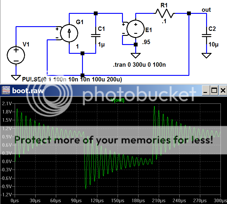
the closer E1 is to 1.00, the less damping due to the bootstrap connection of the op amp which partially cancels the effect of the miller cap C1 - not a exactly trivial compensation situation
LtSpice file:
the closer E1 is to 1.00, the less damping due to the bootstrap connection of the op amp which partially cancels the effect of the miller cap C1 - not a exactly trivial compensation situation
LtSpice file:
G.Kleinschmidt said:Originally posted by Bob Cordell
Hi Glen,
So, if I've got it right, this circuit is just a unity-gain voltage-follower op amp wherein its output is buffered inside the loop by the unity gain output stage. Am I correct?
Not entirely.
Cheers,
Glen
Thanks for the info Glen. Other than the bootstrapping of the op amp supplies, in what way is it "not entirely" just a unity-gain-connected op-amp with the output stage as a power buffer inside the loop?
We'll look forward to your progress in measuring it in a real amplifier. The Devil is always in the details.
BTW, in my amplifier, I routinely got 30:1 reduction in THD at 20 kHz with HEC. But if you can really get 50 or 100:1 at 20 kHz in a real amplifier that is stable with this technique, that's great.
Be careful of instability due to the feedback path formed by the bootstrapping from the output. If that is a problem, you can use feedforward "bootstrapping" from buffered op-amp supply rails formed from the input signal.
Bob
jcx said:G1,C1 op amp model, E1, R1,C2 "unity gain" output stage model:
the closer E1 is to 1.00, the less damping due to the bootstrap connection of the op amp which partially cancels the effect of the miller cap C1 - not a exactly trivial compensation situation
LtSpice file:
Hello,
Of course this a not a good solution, I call it "Munchhausen-Effect"
One time the baron falls in a sump...he pull at his hair to come out😉
Things are much easier if the floating supply is referenced to the input:
http://www.diyaudio.com/forums/showthread.php?postid=1072775#post1072775
Regards
Heinz!
Hi John Curl
Could you tell which mosfets do you use for drivers or which do you suggest?
I was adviced by ilimzn to use IRF710/IRF9610 which in my opinion are perfect for this job and pretty 'complementary'. What do you think?
Could you tell which mosfets do you use for drivers or which do you suggest?
I was adviced by ilimzn to use IRF710/IRF9610 which in my opinion are perfect for this job and pretty 'complementary'. What do you think?
Bob:
Thanks for the info Glen. Other than the bootstrapping of the op amp supplies, in what way is it "not entirely" just a unity-gain-connected op-amp with the output stage as a power buffer inside the loop?
Other than the bootstrapping I didn’t say it wasn’t, I think.
We'll look forward to your progress in measuring it in a real amplifier.
Me too.
BTW, in my amplifier, I routinely got 30:1 reduction in THD at 20 kHz with HEC. But if you can really get 50 or 100:1 at 20 kHz in a real amplifier that is stable with this technique, that's great.
Be careful of instability due to the feedback path formed by the bootstrapping from the output. If that is a problem, you can use feedforward "bootstrapping" from buffered op-amp supply rails formed from the input signal.
OK, when I said that my schematic was a simplified representation, I meant it. In fact, I probably shouldn’t have drawn it the way I did. I over simplified it, but not without good reason - the problem is that this basic circuit is being used to linearise the class A (yes, class A) output stages in a fully differential class A+ power amplifier design, which has class AB stages, not enclosed by global negative feedback, driving the grounds of individual tracking power supplies for the Class A stages. The rails for each opamp are actually derived from part of the driver/buffer circuitry for the Class AB stages, also driven from the same VAS. Also, my preliminary physical prototype uses a pair of NE5534’s, but they will be replaced with a pair of discrete opamp’s if the concept pans out in reality as well as it does in simulation. My main concern here isn't stability, but just how fast I can get the opamp-linearized Class A stages to work, as that will essentially govern how much open loop gain I can preceed them with.
I hope this all makes sense.
Jcx:
Glen;
Well I find the compensation interesting, could you share your earlier apps and references?
OK, earlier apps were predominantly linear high voltage / low current amplifiers for scientific instrumentation. These designs I cannot share. As for the ancient Burr Brown reference, I’m reasonably sure I know where the book is, but you’ll have to wait a couple of weeks, as I’m on my summer break at the moment, without access to it.
Cheers,
Glen
Hi,
I just find bootstrap circuits fascinating. Inspired by some app notes, probably the same as Glen, and by an AKG preamplifier for electret mikes, I designed this buffer. Not yet tried.
I just find bootstrap circuits fascinating. Inspired by some app notes, probably the same as Glen, and by an AKG preamplifier for electret mikes, I designed this buffer. Not yet tried.
G.Kleinschmidt said:
Bob:
Thanks for the info Glen. Other than the bootstrapping of the op amp supplies, in what way is it "not entirely" just a unity-gain-connected op-amp with the output stage as a power buffer inside the loop?
Other than the bootstrapping I didn’t say it wasn’t, I think.
We'll look forward to your progress in measuring it in a real amplifier.
Me too.
BTW, in my amplifier, I routinely got 30:1 reduction in THD at 20 kHz with HEC. But if you can really get 50 or 100:1 at 20 kHz in a real amplifier that is stable with this technique, that's great.
Be careful of instability due to the feedback path formed by the bootstrapping from the output. If that is a problem, you can use feedforward "bootstrapping" from buffered op-amp supply rails formed from the input signal.
OK, when I said that my schematic was a simplified representation, I meant it. In fact, I probably shouldn’t have drawn it the way I did. I over simplified it, but not without good reason - the problem is that this basic circuit is being used to linearise the class A (yes, class A) output stages in a fully differential class A+ power amplifier design, which has class AB stages, not enclosed by global negative feedback, driving the grounds of individual tracking power supplies for the Class A stages. The rails for each opamp are actually derived from part of the driver/buffer circuitry for the Class AB stages, also driven from the same VAS. Also, my preliminary physical prototype uses a pair of NE5534’s, but they will be replaced with a pair of discrete opamp’s if the concept pans out in reality as well as it does in simulation. My main concern here isn't stability, but just how fast I can get the opamp-linearized Class A stages to work, as that will essentially govern how much open loop gain I can preceed them with.
I hope this all makes sense.
Jcx:
Glen;
Well I find the compensation interesting, could you share your earlier apps and references?
OK, earlier apps were predominantly linear high voltage / low current amplifiers for scientific instrumentation. These designs I cannot share. As for the ancient Burr Brown reference, I’m reasonably sure I know where the book is, but you’ll have to wait a couple of weeks, as I’m on my summer break at the moment, without access to it.
Cheers,
Glen
Thanks, Glen, this seems to make sense. Sounds like you are building a version of the amplifier Pioneer did a long time ago in the 70's and was written up in the JAES. It was a really neat concept. The REAL amplifier was a low-voltage Class-A amplifier whose rails were boostrapped by a big Class-AB amplifier driving the "ground" of the floating LV power supply of the Class-A amp. I've always been tempted to build one. So, if I understood, your op amp supplies are bootstrapped in an essentially "feedforward" way by the output of the Class AB amp. Moreover, I guess you could just be using the LV rails that drive the Class A amp for this. This approach means no feedback through the bootstrap and alleviates that stability concern. Is that about right? Cool.
This is not an inexpensive amplifier, right? Each of the Class A amplifiers needs an independent floating LV supply, right? If you are going fully balanced bridging, that means two of these extra floating supplies per channel, right?
Bob
Darkfenriz, the IR devices might work, but it depends on how much current you need. I use J201s and their complement, because I need more current.
Hi all
sorry if this diverts the thread a bit, but in all the debate about MOSFET and bipolar I'd like to know if anyone has tried the SIT transistors developed some time ago.
I've never found anyone who sells these. But they should be as good as tubes - similar output characteristics, mostly second breakdown proof (I would hope) but they seem difficult to find.
Apart from SITs, (no info on their use yet) my recommendation is that bipolars are good for up to about 100W and above 100W maybe MOSFETS are needed.
I'd agree that even the best bipolars from ON Semi still won't have the SOA of a MOSFET at up to ~ 400V. But who wants a build a 4kW amp anyway? Anyone who wants to become deaf?
cheers
John
- Home
- Amplifiers
- Solid State
- Bob Cordell Interview: BJT vs. MOSFET