Hi Charles,
It's getting late here in Louisville - not sure about Boulder though 🙂.
Anyway, you raise a lot of interesting questions that of course I have no clue about what the answer might be 🙂. So I'll keep it brief for now, and we can continue on a fresh note tomorrow.
The cool thing about SPICE and BJTs that many SPICE detractors don't understand is just how well the Gummel-Poon model fits real BJT data, despite its simplicity (compared to some of the exotic MOSFET models). At the same time, many SPICE fanboys don't appreciate just how bad the traditional MOSFET models are when compared to real device data.
Part of the problem is that, in contrast to BJT behavior, MOSFET behavior from the point of view of device physics is kind of compartmentalized with regard to regions of device operation. There's clean expressions for Id vs. Vgs in the weak inversion region, and likewise in strong inversion. But in between, it's a no-man's land. The physics doesn't seem to provide a clear answer when Vgs is in the "in between" region. The clearest information I've found on this is at the web site for the EKV model here. They don't try to get the perfect physics approach, but instead depend on an interpolation approach which, in the transition region, is numerical, not physical. This results in a model that, while not exactly simple, is much simpler than the BSIMx models, and simple enough that it doesn't send you running for the exits like BSIMx does when you read its docs.
Anyhoo, a reasonable description of when the transition from exponential to square law behavior takes place is "somewhere near the threshold voltage Vto". When trying to get models that agree numerically with actual device date, one wants to vary parameters so that in the transition region, the real and simulated device behavior match as closely as possible. But this is just stating the obivous.
Yet, in spite of all the uncertainty of MOSFET modeling, it's clearly wrong to assume that the drain current is identically zero when Vgs is below the threshold voltage. That's the trap that Self implicitly fell into by blindly trusting the traditional SPICE MOSFET models.
Hi, Mr. Hansen,
I've been thinking alot about this gm-discontinuity at crossover area, and I still can't think for a better solution (than what we can read in patents, papers). Making "optimal bias" can give the best from the worse, but still don't make it smooth gm continuity. Runs as much classA as possible seems to be a better answer, but in practical it will be limited by how much dissipation is allowed. It's not practical if we make high-rail voltage power amps. I've also made and compared EC and classA output stage (with the same front end), the classA sounds better than the EC option. This is difficult, how to get a continious gm at crossover area. How to "trick" the output transistor so they gives continious gm, if possible, with reasonable heat dissipation.
This solution (incidentally it is also by NP 😀, patent#5,343,166) seems to be one elegant answer.
With the current RET bipolars where low Vce don't make much different, we can make full use of this principle. For mosfets it is quite limited, because mosfets run better at high Vds.
The principle is to have the output transistors 11-13 runs at high bias, but at low voltage. I've seen a commercial product runs point 21 to 15 plus 15 to 23 only 15V (only 7V5 for each NPN-Vce and PNP-Vce). There's also a schematic around here that have 7A forced current for current source 33. 11-13 can experince smooth gm transistion, but at low heat expense, because the Vce is low. But we have to make a floating secondary PS, and additional casocode transistors (17-19) fixed cascoded towards output node.
It also don't have feedback like EC (which you dont like 😀). What do you think about this?
Attachments
anatech said:Hi Klaus,
In my experience, this increases distortion. I've been matching outputs (and other parts) for years. Some designs are more sensitive than others. Of course, this may just mean that some designs commit larger evils that swamp out mismatch effects.
On Semi figures that your output stage THD could be reduced as much as to 10% it's previous level (before feedback) simply by matching the output transistors. They have "characterized" their new series of audio output transistors for distortion performance. Their figures are for the no feedback case to remove circuit variables.
So finally, after years of defending my position, On Semi came out and verified my practices. 😀 It is a pain though, although the new parts are so much better in device spread than they ever were before.
-Chris
Chris,
I think this idea should be looked at more closely. I read you: you advocate matching the two halves (N & P) halves of an output stage for obvious reasons.
But this idea is something else: Have, say, several output stages in parallel (and each can have matched devices), and let them transition through xover at different output levels. Something like Self's new class X (?) which offsets that crosover in order to avoid xover at very low signal levels, but instead of offsetting it at a new point away from zero, spread it over a range.
Jan Didden
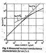
weak inversion
Hi Andy,
When I was asleep, you have saved me a lot of work by explaining some basic properties of power MOSFETs to Charles Hansen. Thank you very much!
And Mr Hanson,
First, allow me to express my displeasure with your attitude. Right from the beginning I pointed out how important it is to take the weak inversion into account. I don't blame for not knowing what the weak inversion implies (although....). But I can't stand it if someone joins in a discussion without having the faintest idea what it is all about, the more so as it takes little effort to google it first (84,800 hits!) and then make a comment.
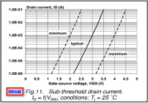
Second, you're still a bit skeptical. Why? I've clearly stated that my models are based on the data sheets and real measurements, see post#2465. Normally, this should suffice. In this case however, I hope I can convince you with more "official" data from Philips (now NXP), which clearly shows an exponential relationship between Id and Vgs, up to about 100mA.
Cheers, Edmond.
Hi Andy,
When I was asleep, you have saved me a lot of work by explaining some basic properties of power MOSFETs to Charles Hansen. Thank you very much!
And Mr Hanson,
First, allow me to express my displeasure with your attitude. Right from the beginning I pointed out how important it is to take the weak inversion into account. I don't blame for not knowing what the weak inversion implies (although....). But I can't stand it if someone joins in a discussion without having the faintest idea what it is all about, the more so as it takes little effort to google it first (84,800 hits!) and then make a comment.
Second, you're still a bit skeptical. Why? I've clearly stated that my models are based on the data sheets and real measurements, see post#2465. Normally, this should suffice. In this case however, I hope I can convince you with more "official" data from Philips (now NXP), which clearly shows an exponential relationship between Id and Vgs, up to about 100mA.
Cheers, Edmond.
Attachments
Hi Estuart,
do you conclude that the graphs of Id vs Vgs are exponential because the plots are straight lines on log/lin scales?
Can you check the originals and confirm if or if not the plots are straight or slightly curved?
If there is slight curving in the Id vs Vgs plots, if this sufficiently insignificant that it can be ignored in this discussion?
When the Id vs Vgs transitions to the square law region, what should the plots look like?
Edmond
The effect of exponential transfer function in FETs is known for years. See below.
From the same Baxandall paper 29 years ago: 'One would not expect that the transfer characteristics for an actual FET to be quite precisely parabolic. Consequently, even without negative feedback, harmonic components in addition to second harmonic must be expected to appear in some extent.'
If Charles didn’t find this region (and the correspondent uneven changes in gate capacitance) in his measurements thus this phenomena has the secondary/negligible effect for his design
p.s. watch your tone please
Attachments
Hi Jan,janneman said:Chris,
I think this idea should be looked at more closely. I read you: you advocate matching the two halves (N & P) halves of an output stage for obvious reasons.
But this idea is something else: Have, say, several output stages in parallel (and each can have matched devices), and let them transition through xover at different output levels. Something like Self's new class X (?) which offsets that crosover in order to avoid xover at very low signal levels, but instead of offsetting it at a new point away from zero, spread it over a range.
yes, that was my thinking, smoothing by spreading (and it also has benefits for the power supply, smoother transition to the half wave rectifying action).
It would mean also seperate bias spreaders and temp compensation (and offsets, maybe) for each pair (ThermalTraks come to mind for this), for that one can choose bias and Re freely for each pair to have some "local optimum". In the back of my head are also those graphs in the search for the optimum bias for lowest 7th harmonic, which came out to be signal level dependent. Of course it might turn out that such a circuitry would be too complicated to be any practical, but at least one might try some sims on this (if were as skilled in this regard as, say, Andy_C is, I would have already done that -- not to mention I'm quite a newbie to discrete amp design, I do mainly op-amp stuff so far).
Regards, Klaus
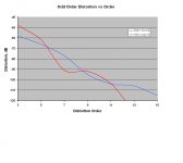
Crossover Distortion vs Order
Below are plots of crossover distortion for two output stages.
Odd-order crossover distortion components are plotted versus the order of the distortion for the two output stages. Both stages are operating at 3V peak into 4 ohms, and this operating level is where the approximate maximum amount of crossover distortion occurs for each.
Which one do you think sounds better?
Cheers,
Bob
Attachments
AndrewT said:Hi Estuart,
do you conclude that the graphs of Id vs Vgs are exponential because the plots are straight lines on log/lin scales?
Hi Andrew,
Yes, I do.
AndrewT said:Can you check the originals and confirm if or if not the plots are straight or slightly curved?
Originals? The graph is from a Philips data sheet, so I don't have the original data. As you can see, the lines are slightly concave, meaning that the relationship is definitely not quadratic, otherwise the curves should be convex.
AndrewT said:If there is slight curving in the Id vs Vgs plots, if this sufficiently insignificant that it can be ignored in this discussion?
It depends on how much curved the line is and in which direction, concave or convex. In this case however, I think we can ignore the slight curving.
AndrewT said:When the Id vs Vgs transitions to the square law region, what should the plots look like?
As I said, convex. Anyhow the data sheet clearly shows that there is quite a large region in which the MOSFET behaves exponential.
I hope I have answered all your questions.
Cheers, Edmond.
Re: weak inversion
Edmond, thank you for your patience. Please know that it has not been my intention to offend you.
Your attached graph from Philips for the IRF640 shows very clearly that the departure from square law occurs at relatively high current levels that will affect the crossover distortion in an audio amplifier. This device is a bit smaller than would normally be used for an audio output stage, so the effect would be even more pronounced in a typical device used for an audio amplifier.
I had always (and apparently mistakenly) thought that this effect only happened at much lower current levels. If I am understanding the attachment to Dimitri's post just below yours, it looks like the departure from square law is occurring at a level of around 5 uA, which was more in line with my understanding. But perhaps this graph is for a small signal device and therefore not applicable to the subject of the output stage. Thank you for clearing this up for me.
My thanks to both you and Andy for explaining this subject in detail and answering my questions. I have benefited from this and am sure that many others have as well.
estuart said:First, allow me to express my displeasure with your attitude. Right from the beginning I pointed out how important it is to take the weak inversion into account. I don't blame for not knowing what the weak inversion implies (although....). But I can't stand it if someone joins in a discussion without having the faintest idea what it is all about, the more so as it takes little effort to google it first (84,800 hits!) and then make a comment.
Second, you're still a bit skeptical. Why? I've clearly stated that my models are based on the data sheets and real measurements, see post#2465. Normally, this should suffice. In this case however, I hope I can convince you with more "official" data from Philips (now NXP), which clearly shows an exponential relationship between Id and Vgs, up to about 100mA.
Edmond, thank you for your patience. Please know that it has not been my intention to offend you.
Your attached graph from Philips for the IRF640 shows very clearly that the departure from square law occurs at relatively high current levels that will affect the crossover distortion in an audio amplifier. This device is a bit smaller than would normally be used for an audio output stage, so the effect would be even more pronounced in a typical device used for an audio amplifier.
I had always (and apparently mistakenly) thought that this effect only happened at much lower current levels. If I am understanding the attachment to Dimitri's post just below yours, it looks like the departure from square law is occurring at a level of around 5 uA, which was more in line with my understanding. But perhaps this graph is for a small signal device and therefore not applicable to the subject of the output stage. Thank you for clearing this up for me.
My thanks to both you and Andy for explaining this subject in detail and answering my questions. I have benefited from this and am sure that many others have as well.
Hi,
I would estimate that that post2486 graph shows a transistion region that extends from 1uA to 50uA.
Some may say it entends even further beyond my estimate.
I would estimate that that post2486 graph shows a transistion region that extends from 1uA to 50uA.
Some may say it entends even further beyond my estimate.
Hi Jan, Klaus,
Interesting. One thing to watch out for though. Since many pairs are needed (I'm guessing three minimum), there would be the desire to use lower powered parts in smaller packages (like MJE1503x types). Since they are smaller, they may also be faster. You want to test one parameter at a time to see what the true differences are.
-Chris
Yes (and that is one reason I'm so happy with the new On Semi parts), but I've always sensed a smoother quality of sound when each polarity is matched to each other. I agree that this should be examined since my findings are only valid for the circuits I am familiar with. By purposely modifying the crossover points we may end up with lower distortion. You may still require matched transistors so they behave the way they are intended.I read you: you advocate matching the two halves (N & P) halves of an output stage for obvious reasons.
Interesting. One thing to watch out for though. Since many pairs are needed (I'm guessing three minimum), there would be the desire to use lower powered parts in smaller packages (like MJE1503x types). Since they are smaller, they may also be faster. You want to test one parameter at a time to see what the true differences are.
-Chris
estuart said:You're right, MOSFETs, need more corrective feedback. My early designs were also equipped with BJTs, but because of my fears of the "hole storage effect" and second break down issues, I switched to MOSFETs.
Hello Edmond,
It's funny (in the ironic sense of the word) that you and I have been moving in opposite direction. My first commercial amp was all MOSFET because I wanted to avoid minority carriers and the "hole storage effect". I even tried to use Schottky rectifiers to carry this idea through the entire amplifier. (It turns out that it is nearly impossible to use Schottkys for high current applications -- they cannot withstand the surge current required to charge a large bank of capacitors.) When the Schottkys didn't work out, I even considered using MOSFET's as synchronous rectifiers to avoid the "evils" of minority carriers. (In the end I "compromised" the design and used ultra-fast conventional rectifiers.)
But as part of consulting project, I designed an amp with a BJT output stage. It performed so well (on the bench and in the listening room) that I started doing more and more investigations into BJT circuits. My current power amplifier designs only use FET's (junction FET's) in the input stage (to avoid the necessity for a coupling cap) and the rest of the circuit uses BJT's entirely.
I avoid secondary breakdown by using balanced bridge designs. The rail voltages are low enough that secondary breakdown is simply not an issue.
Cheers,
Charlie

anatech said:Another annoying fact is the ML figures their schematics are a deep art and hide them from view by not releasing any, even for service.
One of my spies obtained a schematic of one of their amps -
the audio circuit alone required three D size sheets. My sympathy
to anyone who has to deal with them.
😎
Hi Nelson,
There is no reason for that nonsense, especially in this day and age. Sounds like the Counterpoint manuals where the information has been chopped up finely and spread out over a book.
Either way, the schematic represents the truth of the circuit. It can be compressed as required, or reassembled as in the Counterpoint case.
-Chris
LOL!the audio circuit alone required three D size sheets.
There is no reason for that nonsense, especially in this day and age. Sounds like the Counterpoint manuals where the information has been chopped up finely and spread out over a book.
Either way, the schematic represents the truth of the circuit. It can be compressed as required, or reassembled as in the Counterpoint case.
-Chris
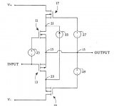
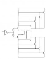
Re: spreading A/B transitions
This brings to mind Barry Thornton's Quintessence amplifier from
the early 70's. I have drawn a simplified version of the
concept topology:
😎
KSTR said:May I ask the experts what you think of speading the individual A/B transitions when using multiple paralleled output devices?
This brings to mind Barry Thornton's Quintessence amplifier from
the early 70's. I have drawn a simplified version of the
concept topology:
😎
Attachments

Nelson Pass said:And here's a variation on the theme:
Interesting. I'm sure you are aware of the latest D Self contraption, I think he called it class X, his design for, was it Musical Fidelity. He basically loads the output stage with a current to one of the supplies to offset the zero current xover away from zero signal xover.
Maybe another variation would be to have multiple parallel output stages, each loaded with a different current to a different supply polarity so each will go through zero current differently. But then how to combine those outputs... Hmm, probably need some diodes somewhere in that circuit...
Jan Didden
- Home
- Amplifiers
- Solid State
- Bob Cordell Interview: BJT vs. MOSFET