Yes, indeed, why choose a device that combines all the worst aspects of the MOSFET and BJT, and none of the benefits, in one package? IGBTs are no good for any sort of linear applications. If you want an active decoupler, then either a MOSFET or BJT will work. If you go with the MOSFET, make sure you include polarity protect diodes, and take precautions against high frequency oscillation: fettit beads on gate leads and gate stoppers. The IGBT in the design here probably poofed due to an undetected high frequency oscillation that can occur well into the VFH rabge.Appreciate your feedback.
- Why choose IGBT while other designs use MOSFET or Darlington? Is IGBT less reliable or I just got a bad part? Should I switch to a MOSFET?
- Does the design dissipate too much heat or cannot handle start up? I tried to turn on heaters for 15 seconds before turn on the power, but not always so.
- Is the heat sink too small? If so, how big should it be?
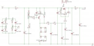
- Every capacitance multiplier is a bit different. However, is this one a good design? I found the use of three 220 uF capacitors in this circuit is a bit excessive. In fact, I now took the IGBT out and connect the capacitors in a simple CRCRC filter. R1 is 82 ohm and R2 is 37.5 ohm. I got B+ at 301V with only 0.5 mV hum at the speaker output. Looks like the capacitor multiplier is not even needed.

jan.didden,
Good question: How do you regulate a power supply?
By regulation, do you mean to 4%, 1%, or 0.01%?
My regulation requires very well regulated power mains, and careful power supply design.
I know I was hardly fair to call my power supplies regulated.
. . . But I did say "regulated".
Just a little tongue in cheek.
Sorry, the original post was a capacitance multiplier, not a regulator.
But the moment the capacitor that follows the rectifier runs out of charge (voltage drops significantly) than the capacitance "multiplier" no longer is able to "multiply" the capacitance.
So far, I have easily resisted the use of capacitance "multipliers".
Large capacitance capacitors are cheap, and the circuit is much more simple than a capacitance "multiplier".
Just my opinions.
Last edited:
How can it oscillate without a feedback mechanism?Yes, indeed, why choose a device that combines all the worst aspects of the MOSFET and BJT, and none of the benefits, in one package? IGBTs are no good for any sort of linear applications. If you want an active decoupler, then either a MOSFET or BJT will work. If you go with the MOSFET, make sure you include polarity protect diodes, and take precautions against high frequency oscillation: fettit beads on gate leads and gate stoppers. The IGBT in the design here probably poofed due to an undetected high frequency oscillation that can occur well into the VFH rabge.
Jan
Well unless you have a direct line to Pacific Power or whoever, that's pie in the sky.jan.didden,
Good question: How do you regulate a power supply?
By regulation, do you mean to 4%, 1%, or 0.01%?
My regulation requires very well regulated power mains, and careful power supply design.
I know I was hardly fair to call my power supplies regulated.
. . . But I did say "regulated".
Just a little tongue in cheek.
But you might check my sig if your serious about it.
Jan
jan.didden,
BJTs are capable of sustaining oscillation at 1.2 x ft. All it takes are parasitic Ls and Cs.
MOSFETs, IXYS regulators, etc. are capable of sustaining oscillation.
Visible feedback path in the circuit (schematic) is not necessary for oscillation to occur.
Just my personal experience.
If it has never happened to you, then consider yourself blessed.
My power mains come off the high voltage power poles that go all the way down the street, and a single transformer feeds only 4 users.
I am blessed to have such good power mains regulation; many others do not have good power providers.
But during start up, although the inrush current is limited, the power dissipation on the MOSFET could go high.The giveaway is the long delay at the base. That limits the rise of Vout and thus the inrush current. It takes more that 10 secs for the load current to get up to 130mA or so.
You could use a simple TO-126 device here with no problems.
Jan
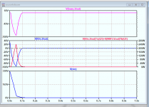
The voltage across C0 will rise close to its maximum after the first cycle. When the voltage across C1 reach 150 Volts, there'll be another 150 Volts applied on the MOSFET together with about 70mA (Suppose the load acting like a resistor). That's over 10W on the transistor.
The green curve shows the power dissipation and the red one shows Vds.
It will reach 14 Watts maximum, while SPP04N80C3 he mentioned can withstand 200 Volts at 250mA, which is 50 Watts.
And I don't think an TO-126 device can withstand that.
KSC5026 is the only device I could found from Mouser which have enough Vceo in TO-126 package. And there's no MOSFET in TO-126. According to its SOA diagram, it can't survive with 14 Watts at 150 Volts. That's almost twice higher than the power dissipation that the Safe Operating Area Diagram showed to us (150 Volts DC Operation, only 50mA is acceptable on KSC5026).
Last edited:
You beat me to that power graph! 😎
And yes, a TO0126 would be a bit optimistic, but the sims show clearly that the device (we still don't know which it is!) is unlikely to blow due to overcurrent.
The dissipation zeros in on about 4W at 15+ seconds, it could be a factor with the wimpy heatsink.
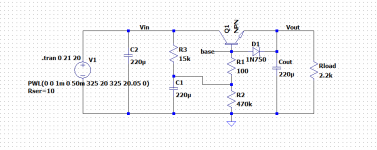
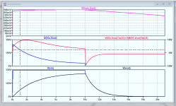
But my money is on exceeding the reverse Vbe/Vge due to absense of a protection zener.
See attached, where the input is switched off in 50ms. First is without protection zener, reverse Vbe is enough to blow it out of the water. Second with a 4.7V zener, all seems fine now.
Jan
And yes, a TO0126 would be a bit optimistic, but the sims show clearly that the device (we still don't know which it is!) is unlikely to blow due to overcurrent.
The dissipation zeros in on about 4W at 15+ seconds, it could be a factor with the wimpy heatsink.
But my money is on exceeding the reverse Vbe/Vge due to absense of a protection zener.
See attached, where the input is switched off in 50ms. First is without protection zener, reverse Vbe is enough to blow it out of the water. Second with a 4.7V zener, all seems fine now.
Jan
Attachments

If it's mysterious it might be a parasitic oscillation. Followers oscillate easily (with their 100% feedback and inductive output impedance) into any sort of capacitive load. This could be ruled in or out with the usual damping strategies, like source/cathode/emitter resistive stops.
All good fortune,
Chris
All good fortune,
Chris
The blown device is an IGBT, so I think you should do simulations with MOSFET or IGBT, which don't withdraw current from C1.You beat me to that power graph! 😎
And yes, a TO0126 would be a bit optimistic, but the sims show clearly that the device (we still don't know which it is!) is unlikely to blow due to overcurrent.
The dissipation zeros in on about 4W at 15+ seconds, it could be a factor with the wimpy heatsink.
But my money is on exceeding the reverse Vbe/Vge due to absense of a protection zener.
See attached, where the input is switched off in 50ms. First is without protection zener, reverse Vbe is enough to blow it out of the water. Second with a 4.7V zener, all seems fine now.
Jan
High Voltage BJTs always have a low current gain ratio, which will affect the stability of the voltage across C1.
With a power transistor whose HFE=50, there'll be about 3mA base current, and the output voltage will drop a lot.
According to my simulation, I can't see any reverse voltage on Base to Emitter. And I think it's due to your setting error.
It's because your Voltage Source will discharge your C2 at a speed of shifting the Voltage Source into a 10 Ohms resistor.
C1, which supplies the Base Voltage in your schematic, will be discharged extermely fast together with C2 through Base to Collector Junction and Base series resistor, which are much much much faster than they should be discharged. And they'll never been discharged through such paths.
IN REAL AMPLIFIER PSUs, your rectification circuit and transformers will not act like a 0 Volts Voltage Source with 10 Ohms internal resistance after turned off. They act like there's nothing after turned off. So what you should change in your simulation is to programme a time delay disconnecting of the Voltage Source, instead of a time delay change in voltage. 😵
You'll see more astonishing results if you forgot setting the internal resistance of the voltage source😆
Last edited:
Good points. I don't know if it is an IGBT, the OP has not been clear about that.
I agree with you that the input voltage drop will not be so fast in real rectifier situation.
In the end, its all about what drops fastest - input or output.
If input drops faster than output there's a change for reverse biasing the B-E (G-E?) junction and/or C-E junction.
Most designers use reverse diodes across the C - E and output to avoid this.
Jan
The input will never drop faster than output unless your main capacitor goes shortcircuit.Good points. I don't know if it is an IGBT, the OP has not been clear about that.
I agree with you that the input voltage drop will not be so fast in real rectifier situation.
In the end, its all about what drops fastest - input or output.
If input drops faster than output there's a change for reverse biasing the B-E (G-E?) junction and/or C-E junction.
Most designers use reverse diodes across the C - E and output to avoid this.
Jan
The reason why your simulation has such error is because you're simulating the circumstance of main capacitor C2 shortcircuit for 50ms. You're not simulating an interruption of AC line.
But why some LDOs have similar designs? A diode from output to input?
Just thinking about the current flow. Where can they go?
The electricity storaged inside C2 has only 3 ways to go.
1. C2's leakage current.
2. The pass transistor to load.
3. R3, C1, and R2, which formed a Low Pass Filter.
C2 can't be discharged from its left side in your schematic in a real amplifier.
But the circuit of LDOs can. If there's no load after the LDOs and there's a heavy load before the LDO, the voltage across the capacitor before LDO will drop fast while the capacitor after the LDO will not. It's in situations like this that you need the diode reverse to the LDO. The manufactures need to consider this for they don't know how users will apply them, but you can see all schematics by yourself. You don't need it here, because the main path for C2 to discharge is going to load through the pass transistor.
And you'll never need such designs when using MOSFETs, because the body diode is there. The body diode of a MOSFET is several times stronger than an external 1N4007. 😵

Post #1 (from "OP"):I don't know if it is an IGBT, the OP has not been clear about that.
Says "IGBT" repeatedly. The part # lists as a IGBT. The CGE pinout looks like an IGBT. I was assuming it was an IGBT. (Which is beyond my experience...)After a few hours playing, the IGBT chip blew (shorted). ..... The actual supplied part for Q1 is FGA25N120, which is a 1200V, 25A NPT Trench IGBT with build-in protective diode.
...voltages at C, G, E were 314.5, 305.2, 292.7V. The amp consumes about 140 mA. So the IGBT is dissipating around 3 watts.
Why choose IGBT while other designs use................
I built an SE amp using IXTH6N50D2 500V 6A depletion MOSFETs... They are configured as followers and idle at 25V@2A in my design but are driven by 6P3S tubes.Hi Gerrit, can you name one or more MOSFET suitable for linear operation?
A 12V zener from gate to source failed to protect it from turn on voltages, so I switched to bidirection TVS and all has been fine ever since. I also has a 50W TO220 1R resistor explode so now I'm using a gigantic 40W ceramic job. It only dissipates 4W but it's almost 100°C.
A TO-220 resistor without heat sink can only dissipate 3W at ambient temperature = 25℃. See Rated Power (in free air) in the datasheet.I built an SE amp using IXTH6N50D2 500V 6A depletion MOSFETs... They are configured as followers and idle at 25V@2A in my design but are driven by 6P3S tubes.
A 12V zener from gate to source failed to protect it from turn on voltages, so I switched to bidirection TVS and all has been fine ever since. I also has a 50W TO220 1R resistor explode so now I'm using a gigantic 40W ceramic job. It only dissipates 4W but it's almost 100°C.
https://www.mouser.cn/datasheet/2/418/8/ENG_DS_1773180_D-1951840.pdf
You don't need to choose a "Linear Usage Specialized" MOSFET.Hi Gerrit, can you name one or more MOSFET suitable for linear operation?
I am actually thinking about ditching the original design and use the design Menno van der Veen published in May 2018 Glass Audio.
He chose SPP04N80C3. It is available at Digikey. There is also a isolated version but is in back order.
I guess 800V 4A is enough for the job.
View attachment 1073990
The biggest difference between them could be inferred from the Safe Operating Area chart.
You just need to simulate the power dissipation during power on process of your amplifier. And calculate the DC operating power dissipation limit of the Safe Operating Area.
This is from IPW65R080CFD datasheet.
The four orange lines I've drawn shown four kinds of different limitations of the Safe Operating Area. The lines paralleled with my DC Operating Power Dissipation Limit line are due to transient thermal resistance of the package.
Calculate the DC operating Power Dissipation Limit. Compare the value to your simulations. Then you'll know whether it's safe to choose such MOSFET.
The model I choose can dissipate 400 Watts safely if there's enough heat sink. It'll be safe for your usage. It'll also be safe choosing MOSFET for SMPS like this one.
DC operating Power Dissipation Limit is mainly decided by the size of the die and package.
It was mounted to the main heatsink, not free air.A TO-220 resistor without heat sink can only dissipate 3W at ambient temperature = 25℃. See Rated Power (in free air) in the datasheet.
https://www.mouser.cn/datasheet/2/418/8/ENG_DS_1773180_D-1951840.pdf
Liar Liar pants on fire. Or is it circuit on fire?You don't need to choose a "Linear Usage Specialized" MOSFET.
This is from IPW65R080CFD datasheet.
Any transistor data sheet that shows a purely thermally limited SOA curve is lying. All suffer from some sort of second breakdown effect - MOS , bipolar doesn’t matter. Some MOSFET types have been updated in recent years to reflect this unfortunate reality. Many of the older types were in fact better.
If what was claimed in the data sheets was actually true, there wouldn’t be a problem charging the output caps hanging off a regulator or hum filter. 3T regs “solve” the problem by internally limiting - and with a discrete design you have to do the same. And understand where that limit REALLY is. If you’re not intimately familiar with a particular transistor from prior experience, you just have to TEST it yourself. Since they are constantly changing which types are offered that makes the job a lot harder. The next offering that is rated two amps more and lower Rds/Vce might not handle as much current at 100, 200 volts as the old one did and you cannot just ASSUME it can.
- Home
- Amplifiers
- Tubes / Valves
- Blown IGBT in an EL34 Tube Amp Kit - what is the cause?