With the isolated input of that owon scope, you can check the waveforms by connecting the ground clip to the source leg of the FETs being probed (be careful not to let the ground clip short to the drain). Recheck the waveforms. Are they better with that ground point?
That's a strange looking drive signal. Post the image of the drive directly on one of the output terminals of the PS driver IC.
Have you calibrated that probe to that scope?
Have you calibrated that probe to that scope?
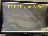
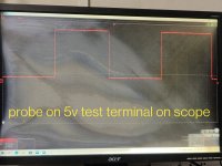
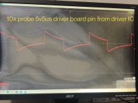
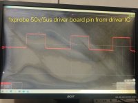
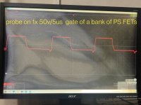
The probe shows a clean square wave on the scope test terminal in both 1x and 10x mode. The waveforms on the PS FETs gates and the driver IC outputs are much more square when the probe is 1x at 50v but I don't know if that is not using the scope properly. Scopeshots posted.
Attachments
-
 IMG_20220812_020908__01.jpg503.9 KB · Views: 44
 -
 IMG_20220812_023436__01.jpg500.6 KB · Views: 48
 -
 IMG_20220812_022703__01.jpg521.1 KB · Views: 49
 -
 IMG_20220812_022936__01.jpg458.5 KB · Views: 46
 -
 IMG_20220812_022256__01.jpg502.7 KB · Views: 52
 -
 IMG_20220812_020419__01.jpg459.4 KB · Views: 51
 -
 IMG_20220812_020050__01.jpg469.9 KB · Views: 46
It looks like you either need to calibrate the probe on 10x or you didn't have a good ground when probing the driver pin on 10x.
Do both your computer and your 12v power supply have a ground pin on their mains plugs?
Are you in the US?
Do both your computer and your 12v power supply have a ground pin on their mains plugs?
Are you in the US?
Not in the US, located in Trinidad and Tobago, West Indies.
Computer and Power Supply are both 3pin plugs with grounding pin.
Are the probes the same from this isolated OWON, and the Hantek and SainSmart USB scopes I had before? One of the OWON probes was not able to calibrate to a completely flat square wave on the 5v test tab.
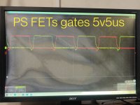
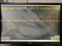
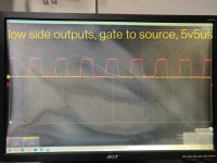
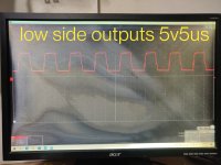
I used an old probe to scope the PS FETs but cannot do the same to the outputs as the amp goes into protection when the probes are connected Gate to Source on both high and low side outputs at the same time. Using one probe, the low side shows fine on one Scope trace, but the high side affects both Scope traces.
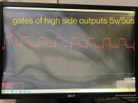
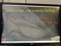
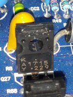
I don't think there is a problem in the Power Supply of this amp but I suspect there may be an issue with the output drive. The readings on the output drivers (C2814) legs from the gate resistors of the high side are suspicious as compared to those of the low side.
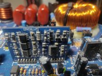
What output IC is used on this driver board?
Computer and Power Supply are both 3pin plugs with grounding pin.
Are the probes the same from this isolated OWON, and the Hantek and SainSmart USB scopes I had before? One of the OWON probes was not able to calibrate to a completely flat square wave on the 5v test tab.
I used an old probe to scope the PS FETs but cannot do the same to the outputs as the amp goes into protection when the probes are connected Gate to Source on both high and low side outputs at the same time. Using one probe, the low side shows fine on one Scope trace, but the high side affects both Scope traces.
I don't think there is a problem in the Power Supply of this amp but I suspect there may be an issue with the output drive. The readings on the output drivers (C2814) legs from the gate resistors of the high side are suspicious as compared to those of the low side.
What output IC is used on this driver board?
Attachments

Last edited:
I think it uses standard probes but the BNC connector is insulated (for safety) on the OWON.
You only have one isolated ground. You can't use two different ground points. Use only one probe at a time.
From what I have, the ZNCM_HP uses 21844s. This board likely does as well.
Check the high-side by connecting the ground clip to the source leg and the probe tip to the gate. Do NOT let the clip short to the high-side drain.
Are the outputs in the amp?
I think it looks OK. The step in the high-side is a bit more than I'd expect but if the FETs aren't heating up at idle, it's likely normal.
Check the gate resistors to confirm that they're within tolerance.
Check the gate resistors to confirm that they're within tolerance.
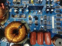
Gate resistors were replaced with same value as original, 22ohms as well as replacing all 8 IRFP260M. I will reinstall the board and test it but I remember the output inductor was the hottest component on the board, but the whole output side of the amp heatsink was hot. Should I try a different value gate resistor for the amp to run cooler?
All semiconductors were purchased from Mouser Electronics except the gate resistors, they were purchased locally but read within tolerance and haven't had any problems with parts from that supplier.
EDIT: Actually, the gate resistors for the outputs were not changed as they were undamaged and read within tolerance. Should I change the gate resistors? I changed all the outputs.
EDIT: Actually, the gate resistors for the outputs were not changed as they were undamaged and read within tolerance. Should I change the gate resistors? I changed all the outputs.
If they read within tolerance, I wouldn't change them.
I'd do as you planned and see if the heatsink still runs hot.
I'd do as you planned and see if the heatsink still runs hot.
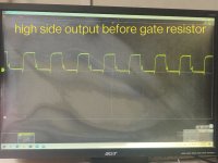
Reassembled the amp and had it running for12-15 minutes and the is about 7-second-touch hot to where I have to let go. I can put my finger on the output clamps without any discomfort as they are not really hot, just a little warm but the chassis/heatsink on that side of the amp is pretty warm. The waveform of the high side outputs is not as clean as the low side. The high side is where the shorted output was...
Attachments

The clamps are not conducting much heat because they're getting their heat through plastic.
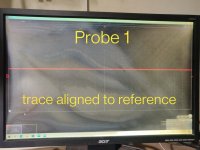
Align all of the grounds (cursors) and the trace to the reference line on the scope and re-check the high-side, on both sides of the gate resistor.
Align all of the grounds (cursors) and the trace to the reference line on the scope and re-check the high-side, on both sides of the gate resistor.
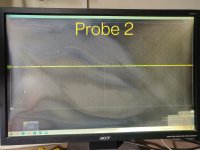
Probe 2 (yellow) has the cursor and trace aligned to each other, but Probe 1 has the trace a little higher than the cursor and I don't know how to align them. I used Probe 2 to scope the high side drive before and after the gate resistor at 5V/5us.
Attachments
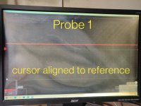

Isn't there a way to align the cursors and the trace?
Does this amp have drivers between the driver IC and the output FETs?
If so, what are they?
Does this amp have drivers between the driver IC and the output FETs?
If so, what are they?
What's the resistance from the emitter of the drivers (either one) to the source leg of the output FETs?
Do you see a pulldown resistor that connects between those two points?
Do you see a pulldown resistor that connects between those two points?

- Home
- General Interest
- Car Audio
- Blown DS18 PRO-KA5000.1D