Hello SandyK
I did noted what he told me, here it is, but I don't know much;
----It turns the damping into quadrature at AF frequencies and thus makes crossover distortion worse because the amp is no longer capable of phase linearly controlling itself at high AF.----
Gaetan
I did noted what he told me, here it is, but I don't know much;
----It turns the damping into quadrature at AF frequencies and thus makes crossover distortion worse because the amp is no longer capable of phase linearly controlling itself at high AF.----
Gaetan
Hi,
re post 98 schematic.
the VAS current is approx 4mA.
The maximum output current from the VAS to the driver bases is approximately +-4mA.
Have you looked at substituting a more realistic reactive load in lieu of 8r0 on the output?
I wonder if a two stage EF gives sufficient current gain for high peak current demand, when a low VAS current is designed into the amp.
Hi AndrewT,
I tried 2ohm resistive load, it should be bad enough Even worse than the worst reactive models: these are useful to measure things such as the worst case dissipation in devices, resistors, etc etc. But the heaviest current (current, not power dissipated in devices) occur when the load is resistive and very low.
Yes, we all know about Cordell and Otala work about worst case loudspeaker current: Self cites the 6.6x factor with respect to an 8ohm resistor. A 2ohm resistor represents a CTF of 4, not far from worst case (of course this isn't an amp for continous 2ohm duty!).
Problems start to appear at about 300W on 2ohm, a power level that probably will never be met, with limitations from the PSU.
Of course I agree with you, I feel not so confident with 4mA VAS current, you're probably right, in practice (in the prototipe) I probably will have to increase current a bit, at least 10mA.
AndrewT said:Hi,
re post 98 schematic.
the VAS current is approx 4mA.
The maximum output current from the VAS to the driver bases is approximately +-4mA.
Have you looked at substituting a more realistic reactive load in lieu of 8r0 on the output?
I wonder if a two stage EF gives sufficient current gain for high peak current demand, when a low VAS current is designed into the amp.
I tried 2ohm resistive load, it should be bad enough
Even worse than the worst reactive models: these are useful to measure things such as the worst case dissipation in devices, resistors, etc etc. But the heaviest current (current, not power dissipated in devices) occur when the load is resistive and very low.Yes, we all know about Cordell and Otala work about worst case loudspeaker current: Self cites the 6.6x factor with respect to an 8ohm resistor. A 2ohm resistor represents a CTF of 4, not far from worst case
(of course this isn't an amp for continous 2ohm duty!).Problems start to appear at about 300W on 2ohm, a power level that probably will never be met, with limitations from the PSU.
Of course I agree with you, I feel not so confident with 4mA VAS current, you're probably right, in practice (in the prototipe) I probably will have to increase current a bit, at least 10mA.
is that why you chose 2sa/c for the VAS & CCS?I probably will have to increase current a bit, at least 10mA.
If the simulator thinks that the gain droop can cope with 2r0 then that is worse than my 8ohm*0.35 that I have recently started to use.
Transient signals into reactive loads needs gains of about 100 and 40 from the driver and output to generate 16A from 4mA. That is about 32Vpk if the 2r0 is a good modeler of your amplifier's drive ability.
But can your output device achieve 8Apk with 200mA of base drive?
Can the drivers give out 2*200mA for a base drive of 4mA?
I suspect not.
Hello friends,
If you're asking why TO126 devices instead of TO92 or similar, yes that's a reason, I plan to heatsink them. The Vbe multiplier is also TO126 because it's easier to mount on the same sink of the drivers (not the outputs).
2SC5200 have very good gain linearity, and so does 2SC3421. Yes, the simulator is a bit optimistic, of course: in real life probably I would increase VAS buffer current and live with less than 300W on 2ohm, which doesn't bother me
Well, BD139-16 has a minimum guaranteed gain of 100, even at 4mA. Selecting good devices from a batch (original Philips) shouldn't be a problem. 2SC5200 has (at 8A Ic) a gain of about 60-80, so for clipping on 2ohm I need less than 2mA from the VAS buffer. I wouldn't use 2mA loading with only 4mA current in real life, I'll still prefer 10mA quiescent current, but hey, this value of current gives lowest distortion in SPICE. One can choose to trust not SPICE in distortion analysis: I choose (based on readings and little experience) to trust it, especially in those areas where little modifications involve only a resistor change, not redesign of the whole circuit.
And of course, the design is still to be tested. I will write it in te PDF: people should not try to build it now, I'm sorry if anyone misunderstood.
I would agree with you, certanly. The way I connected it, when the load is too heavy the output sticks to the negative rail, since I will provide a DC output control it shouldn't be a problem, but I think it's better the way you suggest. That way, the output simply clips, but I don't think it's enough to keep output devices into SOA: I tried increasing R80 to 100ohm, it barely works. Suggestions?
AndrewT said:is that why you chose 2sa/c for the VAS & CCS?
If you're asking why TO126 devices instead of TO92 or similar, yes that's a reason, I plan to heatsink them. The Vbe multiplier is also TO126 because it's easier to mount on the same sink of the drivers (not the outputs).
If the simulator thinks that the gain droop can cope with 2r0 then that is worse than my 8ohm*0.35 that I have recently started to use.
2SC5200 have very good gain linearity, and so does 2SC3421. Yes, the simulator is a bit optimistic, of course: in real life probably I would increase VAS buffer current and live with less than 300W on 2ohm, which doesn't bother me
But can your output device achieve 8Apk with 200mA of base drive?
Can the drivers give out 2*200mA for a base drive of 4mA?
I suspect not.
Well, BD139-16 has a minimum guaranteed gain of 100, even at 4mA. Selecting good devices from a batch (original Philips) shouldn't be a problem. 2SC5200 has (at 8A Ic) a gain of about 60-80, so for clipping on 2ohm I need less than 2mA from the VAS buffer. I wouldn't use 2mA loading with only 4mA current in real life, I'll still prefer 10mA quiescent current, but hey, this value of current gives lowest distortion in SPICE. One can choose to trust not SPICE in distortion analysis: I choose (based on readings and little experience) to trust it, especially in those areas where little modifications involve only a resistor change, not redesign of the whole circuit.
And of course, the design is still to be tested. I will write it in te PDF: people should not try to build it now, I'm sorry if anyone misunderstood.
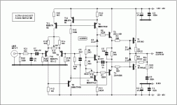
BV said:schematic in post 98
Incorrect conection of Q72 (positive feedback). Colector should be conected to base Q68.
I would agree with you, certanly. The way I connected it, when the load is too heavy the output sticks to the negative rail, since I will provide a DC output control it shouldn't be a problem, but I think it's better the way you suggest. That way, the output simply clips, but I don't think it's enough to keep output devices into SOA: I tried increasing R80 to 100ohm, it barely works. Suggestions?
THD @20kHz vs. VAS buffer current (keeping output stage quiescent current the same):
4mA quiescent current in the VAS buffer (R5: 150ohm)
Vin 0.14Vpk (1W on 8ohm): 1.24E-2
0.3Vpk: 1.48E-2
0.7Vpk: 1.51E-2
1Vpk: 1.43E-2
1.3Vpk (clip): 7.42E-1
7mA quiescent current (R5: 68ohm, less results in the same current )
Vin 0.14Vpk (1W on 8ohm): 1.30E-2
0.3Vpk: 2.55E-2
0.7Vpk: 1.51E-2
1Vpk: 1.44E-2
1.3Vpk (clip): 7.50E-1
Boh...
4mA quiescent current in the VAS buffer (R5: 150ohm)
Vin 0.14Vpk (1W on 8ohm): 1.24E-2
0.3Vpk: 1.48E-2
0.7Vpk: 1.51E-2
1Vpk: 1.43E-2
1.3Vpk (clip): 7.42E-1
7mA quiescent current (R5: 68ohm, less results in the same current
)Vin 0.14Vpk (1W on 8ohm): 1.30E-2
0.3Vpk: 2.55E-2
0.7Vpk: 1.51E-2
1Vpk: 1.44E-2
1.3Vpk (clip): 7.50E-1
Boh...
Hi,
R80 only protects the VAS from excess current.
The CCS is self protecting.
The output stage will need some form of I or IV limiting for protection. This should be supplimented with line fuses to rupture on sustained overload, before the sinks become too hot and then take out the output stage.
Q72 normally only limits when the output stage protection activates. All normal drive should never cause Q72 to trigger.
Yes, for a CFP output stage, the drivers Q19 & Q20 must be coupled to the Vbe multiplier (Q38). Three To92 in a row, glued to a short strip of thick copper or thicker aluminium is normally enough. But 3off To126 bolted will do almost as well.
Hello BV,
I use Orcad Capture, I can't seem to find an option to export the circuit in .cir format. If you know a free program to draw circuits in .cir format, I can provide you a drawing so everyone can do his (or her) own tests.
BTW, I found out that reducing R10 and R11, collector resistors in the CFP driver stage, gives incredible distortion benefits, I almost halved the 20kHz THD... but still there is a THD degradation when you increase VAS buffer current to 9-11mA (from 4mA I'm using now).
BV said:Giaime, can You post here schematic in .cir format? It is simplest way to do some changes..
I use Orcad Capture, I can't seem to find an option to export the circuit in .cir format. If you know a free program to draw circuits in .cir format, I can provide you a drawing so everyone can do his (or her) own tests.
BTW, I found out that reducing R10 and R11, collector resistors in the CFP driver stage, gives incredible distortion benefits, I almost halved the 20kHz THD... but still there is a THD degradation when you increase VAS buffer current to 9-11mA (from 4mA I'm using now).
Attachments
Hi,
q68 sees almost rail to rail voltage when at maximum output. bc546 is not suitable. guaranteed Vce0=60V
it may well survive transient excursions to 70 or 75Vce but hardly recommended.
You have changed r5 but not r80 (that 3:1 ratio I recommended).
The drivers are only up to 7 or 8mA, is it worth going any higher?
Giaime said:Hello BV,
If you know a free program to draw circuits in .cir format,
.cir format is an output from MicroCap simulation program, not a drawing.
You can download a limited version of MC for example here:
http://www.spectrum-soft.com/demodownnew.shtm
Hello AndrewT,
You're right about Q68, I can't seem to find a type that works good in that position. I searched Zetex hi voltage parts, even HF transistors, but they're all in the 50-80MHz ft range, and they show very small phase margin in the amplifier. The best part here seems to be the unobtainable 2SC2240...
Should I return to a cascode VAS, using a high ft device on bottom, and high voltage device on top?
About R80, 33ohm seems a good value to you? It respects the 3:1 ratio.
About the drivers instead (your last phrase), I can't follow you. Do you mean I should try to increase even further drivers current?
AndrewT said:Hi,
q68 sees almost rail to rail voltage when at maximum output. bc546 is not suitable. guaranteed Vce0=60V
it may well survive transient excursions to 70 or 75Vce but hardly recommended.
You have changed r5 but not r80 (that 3:1 ratio I recommended).
The drivers are only up to 7 or 8mA, is it worth going any higher?
You're right about Q68, I can't seem to find a type that works good in that position. I searched Zetex hi voltage parts, even HF transistors, but they're all in the 50-80MHz ft range, and they show very small phase margin in the amplifier. The best part here seems to be the unobtainable 2SC2240...
Should I return to a cascode VAS, using a high ft device on bottom, and high voltage device on top?
About R80, 33ohm seems a good value to you? It respects the 3:1 ratio.
About the drivers instead (your last phrase), I can't follow you. Do you mean I should try to increase even further drivers current?
here's a list of a few medium power VAS transistors:-Giaime said:about Q68,........ but they're all in the 50-80MHz ft range, and they show very small phase margin in the amplifier. The best part here seems to be the unobtainable 2SC2240...
1208/2910
1209/2911
1210/2912
1257/
1360/3423, my favourite
1380/3502
1381/
1405/3599
1406/3600
1407/3601
1415
1476/3782
1477/3787
1478/3788
1480/
1538/3953
1539/3954
1540/3955
1697/4474
1777/4623
1875/4976
low power possibles:
872/1775
sc1815
992/1845
1124/2632
1145/2705
1370/3467
1371/3468
1708/4488
1709/4489
yes, if there is significant improvement going up from 4 to 8mA then try 10, 12, 14mA (500mW) and see what happens. Maybe a big sink and 1W dissipation might be the way to go.Giaime said:About the drivers instead (your last phrase), I can't follow you. Do you mean I should try to increase even further drivers current?
These drivers are providing most of the low power drive before the CFP starts to take over. Check the proportion of output current that comes from the driver and the main outputs as you go from 0.01mW output to 1000mW output (into 8r0).
Hello AndrewT,
Just found a source for 2SC2240-2SA970. We should have fixed the "what bjt" question, now
I've done that, thanks. In SPICE 2SC3281 and 2SA1302 have a little different Vbe (for the same Ic), so driver currents are a little umbalanced, 10mA one side and 15mA the other. But THD decreased, yes, good choice, particulary around milliwatts power levels (well, where we use our amps most of the time...).
I have yet to make other little improvements, mainly fixing a good compromise between low THD and stability, and I think I'm done. THD is still under 0.001% at 20kHz on all power levels.
AndrewT said:
here's a list of a few medium power VAS transistors:-
Just found a source for 2SC2240-2SA970. We should have fixed the "what bjt" question, now
AndrewT said:yes, if there is significant improvement going up from 4 to 8mA then try 10, 12, 14mA (500mW) and see what happens. Maybe a big sink and 1W dissipation might be the way to go.
These drivers are providing most of the low power drive before the CFP starts to take over. Check the proportion of output current that comes from the driver and the main outputs as you go from 0.01mW output to 1000mW output (into 8r0).
I've done that, thanks. In SPICE 2SC3281 and 2SA1302 have a little different Vbe (for the same Ic), so driver currents are a little umbalanced, 10mA one side and 15mA the other. But THD decreased, yes, good choice, particulary around milliwatts power levels (well, where we use our amps most of the time...).
I have yet to make other little improvements, mainly fixing a good compromise between low THD and stability, and I think I'm done. THD is still under 0.001% at 20kHz on all power levels.
are we really expected to believe these simulations?THD is still under 0.001% at 20kHz on all power levels.
AndrewT said:are we really expected to believe these simulations?
Well, I can comprehend your point. With respect to reality, SPICE simulation of THD can give wrong results, for example you can take a wrong turn that in SPICE is better, and in reality it's worse. This is often caused by perfectly matched semiconductors in the simulator, often privileging situations of perfect simmetry that cannot exist in reality.
However, I take another approach: I modify my design based on common design you can find on the net, and basing on common electronic sense.
I would feel very nervous, if SPICE THD analysis privileges a very strange circuit, not-done-before by anyone, which maybe in reality can have stability problems (even thermal), or wouldn't work with real life parts (models aren't perfect).
Instead, I saw that every right application of that electronic "common sense" (let's call it good design practice), and good suggestions from valuable members here in DIYAudio, lead always to a THD decrease in SPICE, without collateral damages such as reduced stability or the like.
It's clear that still exist some thing that "don't look right", such as minimal THD with so low VAS buffer current. They have to be perfectioned in practice, on the prototype.
But all in all the design (as you said, post #91) isn't far from other similar designs, and it seems to feature all the needed to get good performance.
So I won't trust the "absolute" SPICE THD number. But I can trust that, relatively speaking, decreasing THD in SPICE can give good hints of what are the small interations in such designs (after all we're talking about small THD levels, and at those levels the causes of non idealities are not straightforward), and can give you "it works - it doesn't work" suggestions about various things.
The only thing you cannot ask SPICE (this is my electronic professor voice speaking) is to show you how the circuit works, you have to understand it on paper. SPICE is for small improvements and rapid calculations, it's a machine after all, a stupid thing: no better than the humans who designed it.
Maybe I'm wrong. Maybe in reality a beta ehnancer on the VAS (the emitter follower before it) works better than a VAS buffer, I don't know yet, I'm not an amp designer for work (I don't work either
), who knows. After all I'm here to ask you and other amp experts 
- Status
- This old topic is closed. If you want to reopen this topic, contact a moderator using the "Report Post" button.
- Home
- Amplifiers
- Solid State
- Blameless, Dx was wrong, it is a very good amplifier