If you want to check the beta of a transistor, here is a simple, improvised test-jig example:

You need two standard digital multimeters used in the 200mV range, and a supply capable of going <1V.
You adjust the supply to read a suitable voltage on multimeter 1, for example 100mV if you want to make the measurement at 10nA and you read the corresponding base current on multimeter 2 (preferably having a resolution of 20K points or greater).
The rest is just arithmetics.
This method will make the measurement at a low Vce, with Vcb=0 thus quasi-saturation which doesn't help the gain since the Vbe will be 300 or 400mV at this level, but it gives a conservative estimation.
If you add Vbe's in series with the base, you can increase the Vce (use only transistor junctions, not diodes like the 1N4148 which are gold-doped and will drop ~0V at this current level).
Keep the setup compact and well grounded to avoid perturbations, and if you see anomalies, shunt the multimeters with plastic capacitors of 100nF or a few hundreds of nF
Horowitz and Hill actually measured a bunch of BJTs and presented their measured (not datasheet) data on page 504 of "The Art Of Electronics 3rd edition". The horizontal axis is Icollector (log scale) and the vertical axis is current gain (linear scale).
Collector current spans 4.5 decades, from 1E-6 amperes to 5E-2 amperes.
Very high gain NPN transistors with little or no beta-droop at 1 uA (again: measured, not datasheet) included LS301, MMBT6429, 2N5089, 2N5210, 2SC2412
Very high gain PNP transistors with little or no beta-droop at 1 uA included 2N5087, 2SA1016, 2SA1312, 2SB1197KR, 2SA1175
Maddeningly, H&H did not specify the manufacturer of the measured devices, nor did they specify the date codes.
I myself fiddled around with the MPSA18, a high gain NPN device, (here). That transistor had very little beta-droop, but I didn't measure below 15uA of collector current.
I deal with way lower impédances ( like 150R ribbon microphone ) where serious ultra low noise transistors have rbb less than 10R. Low noise op amps have less than 5nV / sqrt Hz noise density
Thanks, 10uA Ic is the low I am looking for.
And wondering about, in the nA realm.
Is this for two different applications? For low noise at 150 ohm source impedance, I would expect a collector current of a milliamp or two, certainly not 10 uA.
For low noise at 150 ohm source impedance, I would expect a collector current of a milliamp or two, certainly not 10 uA
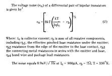
Yes, George Erdi's excellent technical paper "A Bipolar Opamp with a Noise Resistance of less than 50 Ohms" (link) goes over this quite thoroughly. Each of the NPN transistors in the input long tailed pair runs at 0.9 milliamperes of collector current. Beta of these devices is 200, and quite surprisingly, the total base resistance including on-chip wiring and bondwire+package wiring, is rbb = 7.0 ohms ... ... ... not nearly as good as discrete transistors we can buy for $1.50 from Mouser.com. The opamp's datasheet guaranteed maximum input noise density is 1.1 nanovolts per root Hertz.
I snipped out Erdi's equation (1) and attached it below. Notice that Ic appears in the denomimator. Thus an increase in Ic is accompanied by a decrease in noise.
_
Attachments
Last edited:

Yes, different application. For microphone preamplifiers I use ZTX1053A at 2mA Ic.Is this for two different applications? For low noise at 150 ohm source impedance, I would expect a collector current of a milliamp or two, certainly not 10 uA.
Erdi formula shows Shot noise ( 1/Ic term ) + Thermal noise ( rb term ).
Last edited:
I think the formula should be rms'ing those components anyway, not adding them directly... I would normally see the formula as a sum of three terms for voltage, resistance and current, with the source impedance contributing to the latter two terms.
I think that formula is only a rough guide to noise with shorted input, not the best tool in the box...
I think that formula is only a rough guide to noise with shorted input, not the best tool in the box...
The formula hides the sommation of powers.
To deal with noise, one adds powers, or resistances. Voltages do not add, their squares do add.
One can add shot noise and thermal noise because they are white noises in the audio bandwidth. Noise density spectrum is flat.
To deal with noise, one adds powers, or resistances. Voltages do not add, their squares do add.
One can add shot noise and thermal noise because they are white noises in the audio bandwidth. Noise density spectrum is flat.
I snipped out Erdi's equation (1) and attached it below. Notice that Ic appears in the denomimator. Thus an increase in Ic is accompanied by a decrease in noise.
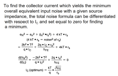
The voltage noise, yes. An increase in IC also leads to an increase in IB, which aggravates base shot noise which contributes to the equivalent input noise current. For a single-transistor input stage, if base and collector shot noise and base resistance thermal noise are the only non-negligible terms, there is an optimum at
re ~= |Zs + rb|/√hFE
or
IC ~= (kT/q)*√hFE/|Zs + rb|
where rb is the base resistance of that single transistor. For a differential pair used in an asymmetrical manner, the optimal collector current per transistor is √2 times as high.
Texas Instruments' application note AN-222 agrees with you, Marcel. They omit the "rb" term, assuming that Zs is much much greater than rb.
Plugging in the Zs number from post #16 of this thread, and plugging in Beta & rb from post #24:
Ic_optimum = (0.026) * sqrt(200)/(150 + 7)
Ic_optimum = 2.34 milliamps
which gives eN = 1.63 nanovolts per root Hertz using a 150 ohm source impedance, a transistor with Beta=200 and rb= 7 ohms, and a collector current of 2.34 mA . The third and final term of the eN_squared expression, completely dominates the other two. The source resistor itself, is the dominant contributor to total voltage noise.
_
Attachments
Last edited:
Some thirty years ago, I made a noise optimization college demonstration circuit. It was essentially a high-gain negative-feedback amplifier with a bipolar input stage and a capacitive source - capacitive so that the source itself would not produce noise and so that current noise would lead to a different spectral distribution than voltage noise. Current noise led to a noise voltage with a -20 dB/decade spectrum across the capacitive source impedance.
The collector current could be changed over a 200:1 ratio by turning a potmeter. A DC loop restricted the bandwidth to 1 kHz on the lower side, and a low-pass filter after the amplifier restricted it to 20 kHz or so on the upper side.
When you turned up the collector current from its minimum, you first heard a sharp hiss getting softer. Then there was a wide region where the noise stayed about equally loud, but it became less sharp, more rumble-like. When you kept turning up the current, the rumble-like noise got clearly louder.
Clearly a wide range of Ic values with near the same low noise.
The optimum Ic from post #29 is interesting theory. However this optimum is of a quite dull shape, so designs are not bound at this exact value.
There are compromises, good reasons to wander around this theoretical Ic ( optimum ).
The optimum Ic from post #29 is interesting theory. However this optimum is of a quite dull shape, so designs are not bound at this exact value.
There are compromises, good reasons to wander around this theoretical Ic ( optimum ).
- Home
- Design & Build
- Parts
- BJT with hight Hfe at very low Ic