Anatech, as already explained, there is no 'cost adder' for extra data in a case like the one we are discussing and its highly unlikely that On would add anthing to the stated prices for adding this data.
Semiconductor pricing, and especially in high volume discretes, does not work like that.
When I mentioned opportunity cost earlier I was reffering to the choice the vendor has to make about where they use their resource - i.e. do they spend one man month on providing a more complete data set for this device or do they put their engineering resource on another project where they will get a better return. Simple economics.
Incomplete data sets for products in the semi industry is not uncommon (quite common I'd say), so I hope no one here views this as On bashing - it would be nice to have the additional characterisation noted earlier.
Sayonara for me on this thread guys.
🙂
anatech said:I must say that On Semi's process appears to be under control. I'm very happy with the transistor part but I haven't checked the diode section.
Funny you should mention that. We did get a batch of parts where the diode forward drop was about 100 mV different than normal. We didn't have enough range in our bias circuit to get them to work right. On Semi tracked it down to a specific date code and replaced the parts immediately. They were very responsive and helpful.
I think it's not so much the fact that there is a problem -- everybody makes mistakes from time-to-time. After all, we're only human! What makes the difference is how those mistakes are handled. And On Semi's response was exemplary. If every supplier was like On Semi, our life would be MUCH easier.
Please note that we are NOT a big customer. I would guess that we buy somewhere between $50,000 and $80,000 per year from them. Too small to go direct, so we have to use distribution. But they still treat us as if we were a $10 million dollar account.
Hi Bonsai,
Hi Charles,
-Chris
Fair enough.Anatech, as already explained, there is no 'cost adder' for extra data in a case like the one we are discussing and its highly unlikely that On would add anthing to the stated prices for adding this data.
They don't even notice my purchases. I'm a tiny player.Semiconductor pricing, and especially in high volume discretes, does not work like that.
That's understood. Business has changed since the 70's for sure.When I mentioned opportunity cost earlier I was reffering to the choice the vendor has to make about where they use their resource - i.e. do they spend one man month on providing a more complete data set for this device or do they put their engineering resource on another project where they will get a better return. Simple economics.
Hi Charles,
For sure!I think it's not so much the fact that there is a problem -- everybody makes mistakes from time-to-time. After all, we're only human! What makes the difference is how those mistakes are handled. And On Semi's response was exemplary. If every supplier was like On Semi, our life would be MUCH easier.
-Chris
Charles Hansen said:
Funny you should mention that. We did get a batch of parts where the diode forward drop was about 100 mV different than normal. We didn't have enough range in our bias circuit to get them to work right. On Semi tracked it down to a specific date code and replaced the parts immediately. They were very responsive and helpful.
I think it's not so much the fact that there is a problem -- everybody makes mistakes from time-to-time. After all, we're only human! What makes the difference is how those mistakes are handled. And On Semi's response was exemplary. If every supplier was like On Semi, our life would be MUCH easier.
Please note that we are NOT a big customer. I would guess that we buy somewhere between $50,000 and $80,000 per year from them. Too small to go direct, so we have to use distribution. But they still treat us as if we were a $10 million dollar account.
Hi Charles,
Your experience here is very encouraging. In my day job we have also had extremely satisfactory response from OnSemi.
Getting devices with diodes off by 100 mV must have been a bit of a jolt! Wow. Is the spread really that large or did they actually make a real mistake, like putting in the wrong diode die? 100 mV makes me think it was the latter.
I'm sure that during routine automated testing of the parts they check the diode drop, but I'm guessing that because there is no spec for it bracketed on the spec sheet, they don't pay attention to the diode drop reading as long as it looks like a diode. If this was indeed an error on their part (as opposed to spread), it could be argued that if they had spec'd it on the spec sheet (even with a fairly wide spread of, say, 60 mV) they would have tested for it and caught their error before they shipped. Just a thought.
On the other hand, if this was really legitimate spread (and they were just being nice to you by replacing the parts), and they had spec'd it, you would have designed the circuit with a wider pot range.
Cheers,
Bob
Bob Cordell said:Getting devices with diodes off by 100 mV must have been a bit of a jolt! Wow. Is the spread really that large or did they actually make a real mistake, like putting in the wrong diode die? 100 mV makes me think it was the latter.
Here is the response we got from the product line manager:
"The cause of the issue was the use of an incorrect diode. We have
modified our test requirements to prevent such an issue from occurring
again."
I believe him, as there is no reason that a MUR120 would have this much variation in it. I would be surprised to see more than about 10 mV variation in a MUR120 for given current and temperature.
On the other hand, I don't know what the heck diode would have such a significantly lower drop. A Schottky would be MUCH lower. A 10 amp part might be about 100 mV lower, but I would imagine that the die size would be a dead giveaway.
Charles Hansen said:
Here is the response we got from the product line manager:
"The cause of the issue was the use of an incorrect diode. We have
modified our test requirements to prevent such an issue from occurring
again."
I believe him, as there is no reason that a MUR120 would have this much variation in it. I would be surprised to see more than about 10 mV variation in a MUR120 for given current and temperature.
On the other hand, I don't know what the heck diode would have such a significantly lower drop. A Schottky would be MUCH lower. A 10 amp part might be about 100 mV lower, but I would imagine that the die size would be a dead giveaway.
Hi Charles,
Thanks for this information. I'm glad to hear it was an out-and-out mistake rather than spread.
Cheers,
Bob
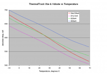
ThermalTrak TCvbe and TCdiode
For those interested, here is a plot of the Vbe of the NJL3281D ThermalTrak BJT Vbe and the Junction drop of its associated diode as a function of temperature from -10C to +70C.
The BJT is biased at a constant 100 mA, deliberately near the region of typical idle bias. The diode is biased at 1/8, 1/4, and 1/2 the value of the BJT.
The diode junction drop is about the same as that of the BJT when it is biased at about 1/4 the current of the BJT.
The temperature coefficient of the BJT Vbe is about -2.14 mV/C, while that of the ThermalTrak diode is about -1.7 mV/C. There is thus a thermal coefficient mismatch of about 0.44 mV/C.
These results seem to be pretty much in line with what Charles said earlier, where he indicated that the diode TC was about -1.6 mV/C.
Cheers,
Bob
Attachments
Bob,
This is most useful-thanks.
Per chance, did you look at the Vbe of the PNP compliment-NJL 1302D?
...Jim
This is most useful-thanks.
Per chance, did you look at the Vbe of the PNP compliment-NJL 1302D?
...Jim
Jim Hamley said:Bob,
This is most useful-thanks.
Per chance, did you look at the Vbe of the PNP compliment-NJL 1302D?
...Jim
Hi Jim,
I haven't yet looked at the PNP in this detailed way over temperature. However, I do seem to recall looking at the PNP Vbe and diode voltage at room temperature at a couple of different currents, and I think they were pretty much the same as this data, at least at room temperature. Knowing what I know now from the construction of the device, I suppose I should not be surprized that the diode is pretty much the same. I'll see if I can dig out those notes and at least confirm that the PNP Vbe was about the same as that of the NPN at room temperature.
Cheers,
Bob
Hi Bob, Jim,
Given that the diode is a separate part of the assembly, I'll bet it's the same part. Why on earth would they change it?
-Chris
Given that the diode is a separate part of the assembly, I'll bet it's the same part. Why on earth would they change it?
-Chris
anatech said:Hi Bob, Jim,
Given that the diode is a separate part of the assembly, I'll bet it's the same part. Why on earth would they change it?
-Chris
Hi Chris,
I agree; that is what I'm assuming.
Cheers,
Bob
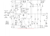
!
I am following this thread from the beginning and at some stage, I
transferred Mr. Cordell's idea of biasing of TTrak devices to Dr. Jagodic.
Here is one possible solution done by him recently as a prototype. I asked
him for permit to publish schematic of this design and he didn't objected
but he wasn't particulary interested neither. His general policy is not to
discus and elaborate his designs in public and for real experts here that is
probably not necessary.
All I can say is that prototype sound amazing and is rock stabile in all
aspects. Some changes were necessary because it was impossible to reduce
total bias under 550mA with original values. Now bias is 150mA per pair and
is rock stabile and drop just 5mA from cold to 70*C. Output ofset is +1,2mV.
My contribution was to design and produce PCB based on Dr. Bora remarks and
requirements.
An externally hosted image should be here but it was not working when we last tested it.
Congratulation to Dr. Jagodic and to you Viktor.
I have done it in a much simpler way, knowing TC of outputs BE junction, NJL diodes and CFP driver at bias current
The bias current is 260mA in the first seconds after startup and it drop to 170mA and stay there regardless of output stage temperature.
http://www.diyaudio.com/forums/attachment.php?s=&postid=1349109&stamp=1194852081
http://www.diyaudio.com/forums/showthread.php?s=&threadid=111756
!
Some general explanation of operation (to the best I understood from few
chats with Dr. Jagodic ):
-Input stage is modified and improved Quinn cascomp according to research
of some Mr. James Woo. Even Mr. Woo version is little more modified and
simplified by Bora
It was very essential to do perfect possible matching of most input PNP
devices to have good results and also of two VAS NPN-s.
-VAS stage is Dr. Jagodic favorite standard differential type but as he
frequently do, it is buffered to keep best performance of good specs of
small transistors in VAS without need to set them in high current and
disipation and to isolate VAS from capacitances of following stages
-predriver/driver & output is according to Mr. Cordell idea, but in
practice it was necessary to be little modified because quiescent current
was more than 500mA and no way to reduce it. That stage also use Baker
clamp.
PCB was real pain in the ***! To keep PCB single sided and tracks
reasonably short, Dr.Bora suggested small accessory board mounted
verticaly on main board and containing majority of output stage
components.
If there is interest, I can post PCB design file and layout file if
someone want to try.
From what I've gathered so far in this thread.....
For Designing an amp with just a single pair (or two pairs) of output transistors, just using the diodes to bias, with a pot or resistor in series with the diodes should be all that's necessary to use the thermaltraks, right?
You don't have to use a VBE mult if you don't have to right?
What about using a resistor in parallel to the diodes instead of series? I'm thinking of making a quick test output stage to compare.
I have the NJL4281/4302 variants. I want to use them in a simple 4 channel setup with a single pair per channel. It would be nice and simple to build if all it needed was 2 output transistors each channel, and the thermal diodes, and a fixed resistor (calculated) to set the desired bias. I wouldn't care if the bias was perfect, but as long as it didn't run away when hot.
a little off topic but........
I like the 5 lead TO-264 package.
It would be cool if they put MOSFETS in the same 5 lead package, but used 1 lead for gate, and used 2 leads each for source and drain to carry more current than a regular 3 lead package.
I like the 5 lead TO-264 package.
It would be cool if they put MOSFETS in the same 5 lead package, but used 1 lead for gate, and used 2 leads each for source and drain to carry more current than a regular 3 lead package.
I don't think two series diodes will give sufficient temperature compensation.EWorkshop1708 said:For Designing an amp with just a single pair (or two pairs) of output transistors, just using the diodes to bias, ..................I have the NJL4281/4302 variants. I want to use them in a simple 4 channel setup with a single pair per channel. It would be nice and simple to build if all it needed was 2 output transistors each channel, and the thermal diodes, and a fixed resistor (calculated) to set the desired bias. I wouldn't care if the bias was perfect, but as long as it didn't run away when hot.
There might be enough but so far I 've only seen 4diodes being used.
The Leach which uses separate diodes in a modified Vbe with 4 in series is overcompensated.
One could possibly hook it up in a diamond buffer style. That is, as a basic scheme, from input via the diode and series resistor to a current source, and from the node below the current source to the base (via stopper), plus the usual emitter R, and probably some caps as AC shunts. And the complementary likewise, mirror imaged. According to various preliminary sims (haven't tested the TT in real life as of yet) there is a combination of current source, series R and emitter R which gives a good operating point, and adjustable amount of compensation tempco, spanning both negative and positive tempcos.
Cons: single wire input (you'd need a good buffer stage ahead of it) and current limit / SOAR protection is a bit tricky to implement. I might suspect problems for a typical class-A/B stage (I simmed only class-A, with occasional class-B transients -- a complementary push-pull cyclotron as the design concept).
- Klaus
BTW: Is there any known info on the response delay (time constant) from the transistor to the diode?
- Status
- Not open for further replies.
- Home
- Amplifiers
- Solid State
- Biasing/thermal compensation of Thermal Trak transistors