ThermalTrak Bias Circuit
Here's an attempt at posting the zip file containing the schematic of the ThermalTrak bias circuit. The models of the BJTs and diodes used are included. The ThermalTrak BJT models are from Andy_c's improved OnSemi models - thanks Andy!
Bob
Here's an attempt at posting the zip file containing the schematic of the ThermalTrak bias circuit. The models of the BJTs and diodes used are included. The ThermalTrak BJT models are from Andy_c's improved OnSemi models - thanks Andy!
Bob
Attachments
ThermalTrak Bias Circuit
Looks like it worked. For convenience, here is the complete post.
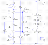
This is a ThermalTrak bias circuit that I came up with that I have been working with. It shows a couple of examples of how the ThermalTrak diodes can be used.
The circuit is in the form of a Class-AB 100 watt output stage in simulation form. The circuit is essentially a triple Darlinton “T” circuit that employs two pairs of NJL3281D – NJL1302D OnSemi devices.
Q1-4 just make up a pair of 10 mA current sources that, in combination with the input voltage source, simulate a typical VAS.
Q5-6 and D1-2 make up a feedback-based bias spreader. D1-2 are the key ThermalTrak diodes that work to establish a stable, temperature-tracking bias. The use of the feedback-based bias spreader, as opposed to a conventional Vbe multiplier, eliminates the influence, drift and uncertainty of the pre-driver and driver Vbe’s in establishing the output stage operating point.
Q7-8 and Q9-10 are the pre-drivers and drivers. D5-6 provide a diode drop of voltage offset to make up for the Vbe of Q5-6. D5-6 and Q5-6 are NOT on the heatsink. The relationship of voltage drop for a given current for D5-6 as compared to Q5-6 is involved in setting the bias current.
The voltage drop across R5-6, caused by R7, sets the voltage that will ultimately appear across the emitter resistors R13-16 (albeit modified slightly by some Vbe differences). In practice, R7 would include the bias-setting pot.
The d.c. feedback from the emitters of Q9-10 to the bases of Q5-6 sets the output stage operating point, and forces a tracking relationship between D1-2 and the Vbe’s of the output transistors.
If D1-2 had the same junction drop as Q13-14, and Q5-6 had the same junction drop as D5-6, you can see that the voltage drop across R5-6 would have to equal the voltage drop across R13-14. Corresponding junction drops are at essentially the same temperature. Note that power dissipation, and thus self-heating, in Q5-6 and D5-6 is quite low. This is how the feedback-based bias spreader works. Although in practice the above-mentioned equalities do not hold perfectly, they are close enough, and net differences are made up by trimming R7 to set the idle current.
The two “extra” ThermalTrak diodes, D3-4, are used between the emitters of the driver transistors to establish the idle current of the drivers while keeping the impedance between the emitters very small, so that the drivers can operate in push-pull to provide turn-on and turn-off current to the output transistors. Keeping the impedance between the driver emitters very low at high frequencies is essentially what is often done with the speedup capacitor. The ThermalTrak diodes make it possible to do this in a d.c. fashion with the necessary precision because they track the output transistor Vbe’s.
Cheers,
Bob
Looks like it worked. For convenience, here is the complete post.
This is a ThermalTrak bias circuit that I came up with that I have been working with. It shows a couple of examples of how the ThermalTrak diodes can be used.
The circuit is in the form of a Class-AB 100 watt output stage in simulation form. The circuit is essentially a triple Darlinton “T” circuit that employs two pairs of NJL3281D – NJL1302D OnSemi devices.
Q1-4 just make up a pair of 10 mA current sources that, in combination with the input voltage source, simulate a typical VAS.
Q5-6 and D1-2 make up a feedback-based bias spreader. D1-2 are the key ThermalTrak diodes that work to establish a stable, temperature-tracking bias. The use of the feedback-based bias spreader, as opposed to a conventional Vbe multiplier, eliminates the influence, drift and uncertainty of the pre-driver and driver Vbe’s in establishing the output stage operating point.
Q7-8 and Q9-10 are the pre-drivers and drivers. D5-6 provide a diode drop of voltage offset to make up for the Vbe of Q5-6. D5-6 and Q5-6 are NOT on the heatsink. The relationship of voltage drop for a given current for D5-6 as compared to Q5-6 is involved in setting the bias current.
The voltage drop across R5-6, caused by R7, sets the voltage that will ultimately appear across the emitter resistors R13-16 (albeit modified slightly by some Vbe differences). In practice, R7 would include the bias-setting pot.
The d.c. feedback from the emitters of Q9-10 to the bases of Q5-6 sets the output stage operating point, and forces a tracking relationship between D1-2 and the Vbe’s of the output transistors.
If D1-2 had the same junction drop as Q13-14, and Q5-6 had the same junction drop as D5-6, you can see that the voltage drop across R5-6 would have to equal the voltage drop across R13-14. Corresponding junction drops are at essentially the same temperature. Note that power dissipation, and thus self-heating, in Q5-6 and D5-6 is quite low. This is how the feedback-based bias spreader works. Although in practice the above-mentioned equalities do not hold perfectly, they are close enough, and net differences are made up by trimming R7 to set the idle current.
The two “extra” ThermalTrak diodes, D3-4, are used between the emitters of the driver transistors to establish the idle current of the drivers while keeping the impedance between the emitters very small, so that the drivers can operate in push-pull to provide turn-on and turn-off current to the output transistors. Keeping the impedance between the driver emitters very low at high frequencies is essentially what is often done with the speedup capacitor. The ThermalTrak diodes make it possible to do this in a d.c. fashion with the necessary precision because they track the output transistor Vbe’s.
Cheers,
Bob
Attachments
Biasing/thermal compensation of Thermak Trak transistors
I'd like to start a new thread to discuss ideas for biasing amplifiers using the inbuilt diodes included in OmSemi's Thermal Trak transitor packages. The simple capacitor in the application note seems a bit simplistic. I was going to use a selected number of these in a diode string in a Vbe multiplier similar to the topology Leach uses so the amp could have the option of using regular transistors and separate diode strings, too, but ideas for
bias schemes strickly for Thermal Traks would also be welcome subject matter.
Leach indicated to me that three diodes were adequate in his scheme, but the forth was added to make the ends of this string come out on the same side of the heat sink. Self believes that intimate contact of the thermal sensor with the transistor could also result in overcompensation, so reducing the tempco may be necessary with the Thermal Traks.
I have make several tests with the Thermal Track trannies, and it works just fine, even though it seems like the bias became a bit unstable.
I used two NPN and PNP as output devices, and had all four diodes in series plus a 100R trimmer to adjust the bias.
Just build it out of head so no schematic, but output stage had same topologi as the Leach amp")
I used two NPN and PNP as output devices, and had all four diodes in series plus a 100R trimmer to adjust the bias.
Just build it out of head so no schematic, but output stage had same topologi as the Leach amp
estuart said:Hi Bob,
Clever clever design, in particular the "improper" use of D3 and D4. I like that kind of tricks.
BTW: any idea why the sensing diode is so large, IF(AV) = 1A, quite hefty for a sensing device.
Cheers, Edmond.
Thanks, Edmond.
I think the sensing diode is so large (same junction drop as the BJT Vbe at 1/4 the current) so as to make things about right at a typical value of bias current. For example, if the bipolar is biased at 100 mA Class-AB idle current, the junction drop of the thermal diode will be the same at a reasonable current of 25 mA. One could argue, I suppose, that a "reasonable" current might be more like a 10 mA value flowing in the VAS. There is also the possibility that OnSemi was deliberately playing some games with delta-Vbe temperature characteristics of junctions operating at different current densities (as is the practice employed in bandgap voltage references).
Anyway, I was a little surprized at the size as well.
Cheers,
Bob
Hi,
if one adopts the dual PNP + NPN Vbe multiplier and then inserts two diodes into each collector leg, like a doubled up version of Leach, what is the effective temperature compensation?
Is it the same as a 4diode Leach or is it equivalent to a two diode Leach but with double the voltage difference?
if one adopts the dual PNP + NPN Vbe multiplier and then inserts two diodes into each collector leg, like a doubled up version of Leach, what is the effective temperature compensation?
Is it the same as a 4diode Leach or is it equivalent to a two diode Leach but with double the voltage difference?
ACD said:Just some info
The Voltage drop over the sensing diode is only app. 0.4 V, and the measurements I have done, shows that this is lower than the Vbe for the trannies. Thats why I added a pot in the sensing diode circuit...........
Hi Jan,
My measurements of ThermalTrak devices have shown Vbe to be about 610 mV at 100 mA IC, while Vdiode is about 610 mV at 25 mA Id. It sounds like you are measuring the diodes at a much lower current.
On that note, I would also point out that using the ThermalTrak diodes in the base circuit of a Vbe multiplier will typically have them running at a rather low current, perhaps on the order of 1 mA.
If you choose to use a Vbe multiplier, I suggest that you place the ThermalTrak diode(s) in series with the emitter of the Vbe multiplier transistor, inside the Vbe muiltiplier loop. This then means that the effective Vbe of the Vbe multiplier transistor will become Vbe_qm + Vj_D, where qm is the Vbe multiplier transistor and D is the ThermalTrak diode. The majority of the VAS standing current will then pass through the ThermalTrak diode.
Cheers,
Bob
Bob Cordell said:
Hi Jan,
My measurements of ThermalTrak devices have shown Vbe to be about 610 mV at 100 mA IC, while Vdiode is about 610 mV at 25 mA Id. It sounds like you are measuring the diodes at a much lower current.
On that note, I would also point out that using the ThermalTrak diodes in the base circuit of a Vbe multiplier will typically have them running at a rather low current, perhaps on the order of 1 mA.
If you choose to use a Vbe multiplier, I suggest that you place the ThermalTrak diode(s) in series with the emitter of the Vbe multiplier transistor, inside the Vbe muiltiplier loop. This then means that the effective Vbe of the Vbe multiplier transistor will become Vbe_qm + Vj_D, where qm is the Vbe multiplier transistor and D is the ThermalTrak diode. The majority of the VAS standing current will then pass through the ThermalTrak diode.
Cheers,
Bob
Good idea. Do you have any notion of the capacitance effects of the long traces to the diodes in this scenario?
AndrewT said:Hi,
if one adopts the dual PNP + NPN Vbe multiplier and then inserts two diodes into each collector leg, like a doubled up version of Leach, what is the effective temperature compensation?
Is it the same as a 4diode Leach or is it equivalent to a two diode Leach but with double the voltage difference?
It does sound interesting to use a dual Vbe, one for each positive and negative half. Might allow a cleaner layout for the diode traces back to the Vbe. Depending on the relative asymmetry of the signals, one polarity can potentially heat up more than the other. Self recognized this issue, but only mentioned in passing that the Adcom GFA-565 was the only evidence he had of its commercial practice. I would think that having two bias adjustment pots would be a detriment, so finding a single adjustment for the total bias voltage would be desirable.
Hi Pooge,
I was going to move some posts over here from the seed thread. My connection is very iffy today so I will not risk it.
What you can do, and I recommend this anyway, simply copy the body of the text you what from the other thread and post it here. You could use the copy function to make it clear who posted what before.
Sorry I can't really help today. Not until the connectivity is cleaned up.
-Chris
ThermalTrak Bias Circuit
I have reposted the circuit description and files here for convenience.
This is a ThermalTrak bias circuit that I came up with that I have been working with. It shows a couple of examples of how the ThermalTrak diodes can be used.
The circuit is in the form of a Class-AB 100 watt output stage in simulation form. The circuit is essentially a triple Darlinton “T” circuit that employs two pairs of NJL3281D – NJL1302D OnSemi devices.
Q1-4 just make up a pair of 10 mA current sources that, in combination with the input voltage source, simulate a typical VAS.
Q5-6 and D1-2 make up a feedback-based bias spreader. D1-2 are the key ThermalTrak diodes that work to establish a stable, temperature-tracking bias. The use of the feedback-based bias spreader, as opposed to a conventional Vbe multiplier, eliminates the influence, drift and uncertainty of the pre-driver and driver Vbe’s in establishing the output stage operating point.
Q7-8 and Q9-10 are the pre-drivers and drivers. D5-6 provide a diode drop of voltage offset to make up for the Vbe of Q5-6. D5-6 and Q5-6 are NOT on the heatsink. The relationship of voltage drop for a given current for D5-6 as compared to Q5-6 is involved in setting the bias current.
The voltage drop across R5-6, caused by R7, sets the voltage that will ultimately appear across the emitter resistors R13-16 (albeit modified slightly by some Vbe differences). In practice, R7 would include the bias-setting pot.
The d.c. feedback from the emitters of Q9-10 to the bases of Q5-6 sets the output stage operating point, and forces a tracking relationship between D1-2 and the Vbe’s of the output transistors.
If D1-2 had the same junction drop as Q13-14, and Q5-6 had the same junction drop as D5-6, you can see that the voltage drop across R5-6 would have to equal the voltage drop across R13-14. Corresponding junction drops are at essentially the same temperature. Note that power dissipation, and thus self-heating, in Q5-6 and D5-6 is quite low. This is how the feedback-based bias spreader works. Although in practice the above-mentioned equalities do not hold perfectly, they are close enough, and net differences are made up by trimming R7 to set the idle current.
The two “extra” ThermalTrak diodes, D3-4, are used between the emitters of the driver transistors to establish the idle current of the drivers while keeping the impedance between the emitters very small, so that the drivers can operate in push-pull to provide turn-on and turn-off current to the output transistors. Keeping the impedance between the driver emitters very low at high frequencies is essentially what is often done with the speedup capacitor. The ThermalTrak diodes make it possible to do this in a d.c. fashion with the necessary precision because they track the output transistor Vbe’s.
Cheers,
Bob
Attachments
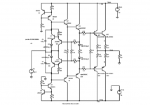
Another ThermalTrak Bias Circuit Variation
The attached circuit is another version of the ThermalTrak bias circuit that I came up with. Some may find this one more attractive. The 1N4001 diodes have been replaced with transistor emitter followers Q11-12 to provide the one-Vbe voltage translation to cancel the Vbe of Q5-6. These emitter followers are powered by stealing one mA from the bias spreader via R10-11. Their collectors are simply returned to the junction of D1-2 to define their collector voltage.
Note that this arrangement buys us one Vbe of additional headroom on each side as compared to the earlier arrangement that employed the 1N4001 diodes.
The second change is the addition of output stage base series resistors R12 and R17 shunted by R18. This combination of resistors causes a slight bias voltage drop of about 20 mV to the output transistors. The purpose of this is to allow the drivers Q9-10 to be biased a bit hotter (now 48 mA) while keeping each output transistor at its desired operating point of 125 mA. Obviously this function can be combined in various ways with base stopper resistors if they are used.
Note that the use of the feedback-based bias spreader is especially advantageous if one is using MOSFET driver transistors at Q9 and Q10, as it will make the bias-setting largely independent of the gate voltage of the drivers.
Cheers,
Bob
- Status
- This old topic is closed. If you want to reopen this topic, contact a moderator using the "Report Post" button.
- Home
- Amplifiers
- Solid State
- Biasing/thermal compensation of Thermal Trak transistors