For now I just added fixed 220r and 10K pot as suggested regarding VBE.. I've noted this as a checkpoint, together with some other adjustments that needs calculation.
Since it's a new drawn PCB, there is a ton of other things that could go wrong when building, faulty PCB layout that could cause all sorts of other problems for example... I have enough powertransistors for one prototype, before new stock mid 2022! 🙁
Since it's a new drawn PCB, there is a ton of other things that could go wrong when building, faulty PCB layout that could cause all sorts of other problems for example... I have enough powertransistors for one prototype, before new stock mid 2022! 🙁
Attachments


Last edited:
I quite new in understanding everything involved in amplifierbuilding, the math behind really start make sense when probing, so for now, my goal is to make the circuit, starting with the single NPN-BIAS as I know this has worked for me before. After this I'll try the PNP also, measuring and understanding it's influence
Non est tantum facilePositioning the sense transistor is an interesting exercise in itself.
You can calculate the thermal impedance path from the output and drivers to ambient, and as the heatsink temperature will not be as great as the junction of the output device (usually the hottest) you would conclude that you need a greater multiple of Vbe than the 4 I suggested, by the ratio of the thermal impedances.
However if you put the bias right next to an output device (such as on the metal can but insulated) 4Vbe's could over-compensate because the output device(s) is/are hotter than the drivers. (Usually).
Putting the sense device on the same heatsink as the driver and output is a compromise that worked for me in many designs. This may explain why the simple multiplier circuit actually works as well as it does.
The actual 'multiple of Vbe' isn't the problem. We have a twiddle pot to set the exact bias current we want under our specified condition.
The problem is what happens when the amp heats up & then cools down. For this we need to match the "thermal gain" ... which is determined by the EXACT positioning and mounting of the sensing device (the BJT in our case) ... to the 'voltage gain' provided by the Vbe multiplier. This also needs to allow for thermal lag as everything heats up and cools down.
I now think Cordell's book has a better chapter on this than Self.
____________________________________________
hcpower, where are you mounting your sensor?
"Non est tantum facile"
but then you go on to describe how it might not be!
Anyone can set the bias current with a Vbe multiplier at a given temperature.
The ratio of the multiplier may not be what is required to hold the bias current constant as the temperature changes. That's the problem.
One approach would be to use a nominal bias, allow the amplifier to run under a controlled condition (measring the heatsink temperature etc) and determining the bias current with temperature ratio.
That will provide some information as to the Vbe multiplier ratio you actually need to do the job, not just setting it at one temperature.
If that ratio is different from the one you started with you will need to modify the circuit.
As I mentioned, Hawksford's current compensation could be used as a means to adjust the ratio while also generating some independence of VAS current.
A large heatsink generally provides a decent thermal lag to smooth short term variations out. Particularly as the transient thermal impedance of a transistor is much lower than the static or "D.C." value, which means perhaps there is less effect of a musical transient than might appear.
But there are additional subtleties too, such as whether a capacitor across the multiplier can charge or not. As it can, that will probably have more influence on the dynamic bias than we would like. For this reason it is better to keep the capacitance, if needed to avoid oscillation, to the minimum necessary.
Last edited:
The chassis will be a Modushop Dissipante 5U/400mm. So lots of heatsink, to provide a decent cooling of the transistors
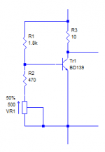
1) WHY do you want a PNP there?any suggestions to implant an 2SA1837 PNP-transistor to this circuit. I want a more stable design.
No special advantage whatsoever.
2) as suggested by many and specifically by Mr Nelson Pass , a transistor junction and matching Vbe multiplier is good enough.
As also suggested above, your main problem is not "electrical" but "thermo-mechanical" , meaning how well sensing transistor junction temperature tracks heatsink temperature.
And that depends a lot on heat sink geometry, mass, and thermal coupling between sensing transistor and heatsink metal.
Some drill a hole if thick enough and put a TO92 transistor "head" inside,often with an drop of thermal grease.
Being a Minimalist, find dealing with a single silicon junction enough, and shudder at your circuit having THREE, which to boot won´t couple equally or well to heatsink .
Fear you add problems without really offering solutions.
You could design a better tracking system by detecting sensor Vbe drop and then non linearly processing that voltage to calculate actual power transistor *junction* temperature, but that is a higher level of complexity solution beyond a regular Forum thread level.
So far we are actually tracking heat sink temperature, not the same.
In fact somebody around here cleverly mentions that in his signature, go figure.
So in a nutshell: I´d go back to the original "transistor+2 resistors" Vbe multiplier Bias and if needed improve thermal coupling.
Nowadays, the current State of the Art.

"1) WHY do you want a PNP there?
I've explained. (but not in the circuit hcpower originally showed)
I don't disagree that a single transistor works OK for a driver/output double.
If you have a triple output stage which is well known to be more difficult to control I recommend the complementary design. It works better than the single device as it allows the precise Vbe ratio needed to keep the bias current stable. In fact it is possible to generate a negative TC of bias current which is not possible with the single device (unless, perhaps, using the Hawksford mod).
Is it worth adding 1 more resistor to make the Hawksford option - no need to use it if not required. (replace with short circuit).
I usually use a TO-126 sense transistor like a BD139 as it is easy to mount, but does need an insulator.
You are not making this easy @john_ellis😉
I published my project in another forum where everyone pointed towards a PNP/NPN-BIAS.... Diyaudio is the first where I'm recommend to leave it as a single NPN/2-resistor network.
I will upload a better schematic when I'm at the computer.. That said, I'm using a knock-off 2SA1837/2SC4793 from UTC in TO-220 packed
Regards
Just curious, what would the other Forum be?
As of why a single humble PN junction is good enough to detect thermal shift, it´s because that´s all it takes.
No need to match power transistor polarity, ALL will have Silicon PN BE junctions,all will drift the same: 2mV per Deg C , so for any give design, you just count how many BE junctions you need to just turn ON and design the proper multiplier: 3:1 ,4:1 , 5:1 , whatever.
It is not much more complicated than that.
Now in a circuit like the one you originally posted:
* WHICH is the sensing yransistor?
* what happens with the other one?
* what happens with the diode?
¨are ll them mounted on the heatsink?
Just one or two? None?
Notice you turned a simple to solve, *one* variable equation, into a complex 3 variable one, with undefined interaction.
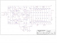
The schematic before I laid my hands on it, is highly inspired by Acurus A250/Aragon 8008. Put the two schematics together, and you'll quickly notice. The thought is to add the power that the 8008 never had. I own an A250 that is highly modded for everyday listening, and most of the new schematic has been experimented in this amplifier without problems..Just curious, what would the other Forum be?
As of why a single humble PN junction is good enough to detect thermal shift, it´s because that´s all it takes.
No need to match power transistor polarity, ALL will have Silicon PN BE junctions,all will drift the same: 2mV per Deg C , so for any give design, you just count how many BE junctions you need to just turn ON and design the proper multiplier: 3:1 ,4:1 , 5:1 , whatever.
It is not much more complicated than that.
Now in a circuit like the one you originally posted:
* WHICH is the sensing yransistor?
* what happens with the other one?
* what happens with the diode?
¨are ll them mounted on the heatsink?
Just one or two? None?
Notice you turned a simple to solve, *one* variable equation, into a complex 3 variable one, with undefined interaction.
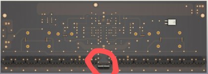
Looking isolated at the Aragon 8008 PCB (Google is your friend), one would realise that Mondial managed to produce am amplifier with 6 drivers mounted with a separate heatsink on the PCB.
Still a single NPN for BIAS though.
Voltage is raised from 70VDC (Aragon 8008) to around 85-90VDC, and will cause ekstra heat. Thereby the bigger heatsinks at the PCB, and bigger heatsink on the amplifier chassis itself when build.
I'll stick to the 2SA1837/2SC4793 TO220 devices as used in the 8008 both at drivers and BIAS.
Sorry!
But there we are. A complementary design has worked better for a triple output than the standard one transistor in my amps.
I also have used a single transistor Vbe multiplier successfully when (as pointed out in other threads) it is on the same heatsink as the driver and output transistors in the two stage EF output (which though your design uses a load of output transistors is essentially that).
The PNP offers a means of adjusting the current in the NPN and reducing the net impedance of the bias regulator.
I suggest the Hawksford option as a peace offering.
This is my recommendation for your circuit because it will compensate for variations in current in the VAS stage as that may drift. I don't know what VAS current you are planning (the circuit component values are not too clear) but as there are no compensating diodes I can see in the VAS bias arrangement (unless I missed something in the constant current sources of the diff input stages) I can imagine the current will drift upwards a little with temperature.
The additional resistor in the collector provides a bigger drop as the current increases. Also the Vbe multiplier ratio is increased a little compared with the standard. Both of these give you an advantage over the basic NPN+2 resistors.I've not attempted to optimise the additional resistor value as that depends on the current. I'm guessing around 10mA.
Attachments
Last edited:
Thanks I'll do so. A second thought also turned out that it would be absolutely stupid not to try the PNP, as this can be easily bypassed in a proto, but fare more complicated to add to a designed PCB afterwardsSorry!
But there we are. A complementary design has worked better for a triple output than the standard one transistor in my amps.
I also have used a single transistor Vbe multiplier successfully when (as pointed out in other threads) it is on the same heatsink as the driver and output transistors in the two stage EF output (which though your design uses a load of output transistors is essentially that).
The PNP offers a means of adjusting the current in the NPN and reducing the net impedance of the bias regulator.
I suggest the Hawksford option as a peace offering.
This is my recommendation for your circuit because it will compensate for variations in current in the VAS stage as that may drift. I don't know what VAS current you are planning (the circuit component values are not too clear) but as there are no compensating diodes I can see in the VAS bias arrangement (unless I missed something in the constant current sources of the diff input stages) I can imagine the current will drift upwards a little with temperature.
The additional resistor in the collector provides a bigger drop as the current increases. Also the Vbe multiplier ratio is increased a little compared with the standard. Both of these give you and advantage over the basic NPN+2 resistors.I've not attempted to optimise the additional resistor value as that depends on the current.
Good day
😕highly inspired by Acurus A250/Aragon 8008. Put the two schematics together, and you'll quickly notice.
Which schematics?
On which post did you show them?
You are doing the asking, you supply the data. 😎the Aragon 8008 PCB (Google is your friend),
😕
Which schematics?
On which post did you show them?
You are doing the asking, you supply the data. 😎
Yes sorry, I know!😉
I'll make a post, everything included when the kids are in bed.
Regards
Ok.... First the inspiration...
The Acurus A250 and Aragon 8008 schematic. Last picture is the Aragon 8008 PCB regarding the layout of drivers and NPN-BIAS in center at the bottom.
Rails in A250 is 85VDC, but often measured above 90VDC in the units I've seen.
8008 is 70VDC
I'll return with my own schematic in next post, with both the new PNP and the original layout
Attachments

Last edited:
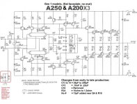
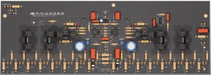
Here is my sche.... 90VDC rails..
The NPN and the NPN_PNP-BIAS setup..
Pic attached is the one with added VBE-pot and PNP to BIAS, in center of the powertransistors
Best Regards
The NPN and the NPN_PNP-BIAS setup..
Pic attached is the one with added VBE-pot and PNP to BIAS, in center of the powertransistors
Best Regards
Attachments
Last edited:
But.... I must admit I think I have enough information to try some different approaches. And I need to buy some books regarding amplifier build 😉
Thanks
Thanks
I think we are actually reading from the same page. 😎"Non est tantum facile"
but then you go on to describe how it might not be!
Anyone can set the bias current with a Vbe multiplier at a given temperature.
The ratio of the multiplier may not be what is required to hold the bias current constant as the temperature changes. That's the problem. ....
__________________
john_ellis, you mentioned you dreamt up your complementary bias network to deal with EF3 output stages. Can you elaborate please.
Where did you mount the 2 sensors?
Did the drivers & pre-drivers share the Heatsink with the outputs & the sensors?
__________________
I used to design amps for a living and my concern was setting bias in production test. That's why I'm prejudiced against EF3 cos there was no way the bias would settle down in 5min.
If your method allows this, I'm interested in EXACT details.
Mike Albinson & Peter Walker told me this was the real reason they invented Current Dumping.
Last edited:
- Home
- Amplifiers
- Solid State
- BIAS network recommendations