Re: TEXAS AMP SCHEMATIC
The closed loop gain of 4.33 is a little low for a power amp!?
What is the purpose of the 1 ohms resistors (it seems a little low to have a real effect)?
LineSource said:
The closed loop gain of 4.33 is a little low for a power amp!?
What is the purpose of the 1 ohms resistors (it seems a little low to have a real effect)?
LOW NOISE WITH LOW IMPEDANCE
I built differential input stages with a 2SK389 matched JFET pair and a MAT03 NPN bipolar matched pair in +/- 12 volt rails, and put the o-scope on the diff-output with the inputs tied to ground and +/- 1 volt to look for noise. With a 1K ohm input resistance, the MAT03 showed less noise. 5ma bias from bipolar/LED current source, resistor pull ups.
In my application there is a 1V D-to-A with a 30 ohm output infront of the power amp. This allows a low 1K ohm input inpedance for the amp.
I would appreciate any shared experience of amp designs using MAT02 and MAT03 low noise bipolar pairs.
I've used the MAT-02 and MAT-03 in designs, but in secondary positions, such as creating a differential current source load, or as a VAS buffer from a previous differential stage. They're quite nice, if a tad expensive, but you do have to observe their current and power handling limits. I can't post that work because it was done for a client.
Now, in principle, there's no reason you couldn't build the diff front end with them, though I usually use matched sets of differential FETs in parallel. It might be worth trying Tektronix's cascomp input configuration; it simulates very well, though I haven't built it up and listened to it. I'd consider it for a non feedback amp front end, considering the possibility of linearization of the diff stage with extended input voltage range.
~Jon
LineSource,
i'm afraid you're nowhere near measuring differences in input noise between those Qs under the described bias conditions
1 KOhm source will give you >4 nV/SQRT(Hz) Vnoise before adding the ib current noise from the MAT while the Vn for those devices should be near 1nV/sqrt(Hz) – the conclusion that the MAT is quieter than the SK fet with 1K input is sufficient proof that the measurement was not good – some of this EE theory stuff actually does get you close to the real world answer, kinda what defines a discipline as engineering
you would need a very sexy low noise, diff amp for your probes to have a chance of seeing the input device noise with any 'scope i've ever used - even allowing for the gain of the input stage which gain is strictly limited with resistive collector load and 12V supply
'scope and probe cmrr limits also require very low noise supply to make this measurement, for a start i would use batteries and ref the 'scope to the collector resistor supply rail and probably build a dedicated 100-1000x low noise op amp gain stage
Added noise is because your second stage current mirror SUCKS noise-wise ;-). Use larger value current mirror degeneration resistors in your design.
What do you mean by "improvement"...what are you trying to achieve with this design?Any suggestions for improvements?
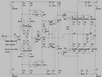
Is the schematic correct? J5/J11 and J12/J9 look asymmetrical.
You should have a cap across R7 to filter RF at the input
R28,R29 - why aren't these current sources?
Why have you chosen to set the current through the diff pairs by means of a common resistor and the turn-on Vgs of the JFETS?
You have a series resonant circuit (C12,L1) across the output; this will create a dead short at 519kHz (as I mentioned earlier in this thread). What are you trying to achieve with this?
traderbam said:
R28,R29 - why aren't these current sources?
What would the benefit be replacing the R28, R29 with cct?
It appears to me that the currents through Q1 and Q11 are modulated, approximately, by the difference in voltage between output and supply rail.
Traderbam, all,
Ok, so the current source gives just better PSRR and stabile current, but is the benefit that big with Q1 and Q11 as EF?
The arrangement around Q1, 4, 11, 12 looks like a diamond buffer too...
Would there be any other benefits using current sources since they are used in diamond buffers too?
Ok, so the current source gives just better PSRR and stabile current, but is the benefit that big with Q1 and Q11 as EF?
The arrangement around Q1, 4, 11, 12 looks like a diamond buffer too...
Would there be any other benefits using current sources since they are used in diamond buffers too?
traderbam said:It appears to me that the currents through Q1 and Q11 are modulated, approximately, by the difference in voltage between output and supply rail.
Based on the schematic, V1 and V2 are different from V3 and V4. Thus, it suggests that V1 and V2 could be well regulated (invariant to modulation of power supply with output voltage)then the current sources may be less essential. However, the current sources would not harm either...
Also,
What is the purpose of R32 in the bias voltage multiplier section?
What is the DC offset at output with no DC blocking caps nor DC servo?
The first and second stage look similar to http://www.borbelyaudio.com/index34.htm
from Borbely (if you remove the mosfets and DC servo from Borbely circuit).
Re: JFETS WITH BIPOLAR OUTPUT
how about control panel>drafting options>color scheme>background> r,g,b = 255, you might also increase line weight too
then try the .op operating point analysis, rather than reading the output text file you can close it and then slide the cursor over the nodes and components to get the dc operating conditions in the lower left corner of the screen
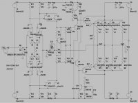
I think you’ll find you need to work on basic bias issues first; J5,9,11,12 can’t be doing anything useful in the present configuration – to bias these fets you would need a large drain current imbalance in the diff stage
Also try plotting input device currents or load R volts for both halves of the diff pair to see if you really have diff pair action – and to look at input stage gm linearity and evaluate what components/topologies actually improve it
LineSource said:Any suggestions for improvements?
how about control panel>drafting options>color scheme>background> r,g,b = 255, you might also increase line weight too
then try the .op operating point analysis, rather than reading the output text file you can close it and then slide the cursor over the nodes and components to get the dc operating conditions in the lower left corner of the screen
I think you’ll find you need to work on basic bias issues first; J5,9,11,12 can’t be doing anything useful in the present configuration – to bias these fets you would need a large drain current imbalance in the diff stage
Also try plotting input device currents or load R volts for both halves of the diff pair to see if you really have diff pair action – and to look at input stage gm linearity and evaluate what components/topologies actually improve it
VAS STAGE CURRENT TOO LOW
jcx - appreciate the comments. The best bias point looked like 700-1000 ohms for the front differential pull-ups, but for the low power supply voltages and 4A class A output bias currents needed, this puts only 200-300 uA running in the VAS stage, which is too low to drive the output stage cleanly. Any suggestions in how to get a few milliamps in the VAS stage and still have ~700 ohms in the front differential stage pull-ups with this topology? This 15V input stage and 12V output stage with 400 ohm pull-ups on the differential puts about 1ma in the VAS , which looks like the minimum acceptable bias. The +/- 15V is also used by the D/A that drives this amp.
jcx - appreciate the comments. The best bias point looked like 700-1000 ohms for the front differential pull-ups, but for the low power supply voltages and 4A class A output bias currents needed, this puts only 200-300 uA running in the VAS stage, which is too low to drive the output stage cleanly. Any suggestions in how to get a few milliamps in the VAS stage and still have ~700 ohms in the front differential stage pull-ups with this topology? This 15V input stage and 12V output stage with 400 ohm pull-ups on the differential puts about 1ma in the VAS , which looks like the minimum acceptable bias. The +/- 15V is also used by the D/A that drives this amp.
Attachments
Linesource,
Current sources - nice. 🙂
Something I'm struggling with is the orientation of some of your JFETs. I'm not sure whether it's the way your simulator draws them or an actual mistake. I'll mention it just in case: J6, J7, J8, J9, J10 and J12 look like their S and D are the wrong way around.
Regarding VAS current, I think 200uA is plenty if you adjust the CCS a little. You have about 10mA bias in Q4 and Q12 and I reckon 10mA bias in Q1 and Q11 is ample. So set CCSs at 10mA. Provided Q1 and Q11 have beta >100 you don't need much to drive them, especially as you have no compensation capacitors, which may cause other problems. 200uA is fine as it stands, may need up to 1mA when you copmpensate it.
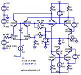
i don't see an obvious advantage of the symmetric input, but if you insist on fet input diff pair why not take advantage of the matched duals and punt on source degeneration - in theory ideal, matched square law devices will have no output distortion in a diff pair
the circuit below uses the fets in the diff pair and bjt for "current mode" manipulations - where bjts excel
the J1,2 fet drain currents are reflected in the folded cascode Q1,2 and the vas is balanced by reflecting J1/Q1 drain/collector current thru current mirror Q3,4,5,6 - the vas outputs Q2,4 being cascoded by Q6,7
1 Meg R10 subs for the 1 ohm load seen thru (100+ hfe)^3 at the input to the triple Darlington output buffer, e1 closes the loop and lets you concentrate on input+vas issues
Q8,9 C2 and R7,8 form a bootstrap cascode of the input stage, reducing simulated 2nd harmonic distortion by ~ 30 dB to nearly equal the -135 dB 3rd harmonic in the sim
i'm not proposing the 2N5484 is the ideal audio input device (or that the models of any of the transistors are valid at these ridiculously low distortion levels), it was however provided with the LT SwCad
Attachments
jcx!how are the voltage of 2nd and 3rd? i don't know db unit.
I think we should try to do with new techique.
I think we should try to do with new techique.
tanh, you really need to know dB to go far in audio electronics
looking at the output of the .four 20kHz V(out) spice statement
2nd & 3rd harmonics are ~1.6e-7 re 6V output ( 2nd & 3rd harmonic amplitude ~ 1 uV with 6V output @20KHz)
the point i take from the sim is that the "asymmetric" single diff pair and the "unbalanced" mirroring of the current to get push-pull output doesn’t show any defect that could reasonably be expected to be improved by fully complementary topologies
so I think it would be more useful to focus on output stage distortions which are much larger than any common input stage’s distortion
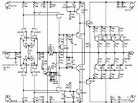
DESIGN 1
jcx..I'll look over your ideas next week and see if I can stitch them to my Class A output stage
Appreciate suggestions for improvements.
Goal 25watts into 1 ohm for > 100db/w resistive speaker...i.e. 1st watt critical
Design 1
+low noise JFETs for front diff + VAS
+VAS uses both differential outputs from front-end for gain + CMR
+single stacked complementary differential input
-low R pull-ups in front diff give compromised bias point
-onlly 1ma in JFET VAS
-servo in signal path feedback loop
Any suggestions for increasing VAS current while keeping diff pull-up Rs high?
Attachments
- Status
- Not open for further replies.
- Home
- Amplifiers
- Solid State
- best topo for 25W class A into 1 ohm resistive load?