MicroBeast single ended cascode PCB. 7 cells populated. 143 mA idle current.
+/- 15 v rails. J113 chrrent source. Gain JFET. J111 cascode.
Output 6.69 v RMS into 70 ohms before clipping.
Fully populated 10-cell Micro Beast single-ended cascoded.
203 mA idle current. + / - 15v rails.
unclippped max outputs at various load resistances
10 ohms, 1.518v RMS 230 mW
30 ohms, 4.41v RMS 650 mW
50 ohms, 6.7v RMS 950 mW

203 mA idle current. + / - 15v rails.
unclippped max outputs at various load resistances
10 ohms, 1.518v RMS 230 mW
30 ohms, 4.41v RMS 650 mW
50 ohms, 6.7v RMS 950 mW

10 ohms, 1.518v RMS 230 mW ---> 152 mA RMS , 215 mA peak
30 ohms, 4.41v RMS 650 mW ---> 147 mA RMS , 208 mA peak
50 ohms, 6.7v RMS 950 mW ---> 134 mA RMS , 190 mA peak
All of them are pretty much within experimental error of what you might expect to see, from an array of (follower + constant current load) cells, running at 203 mA idle current.
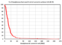
In the present form, it will successfully drive all but the last 2-3% of the 84 headphones in this survey , to 110dB SPL. And oh by the way, 110dB SPL would be way too loud and actually painful.
How to read the red curve: find the point where AC current = 30mA on the horizontal scale, and %Headphones = 17% on the vertical scale. This means: 17% of all headphones surveyed require 30mA or more, to achieve 110dB SPL. It also means: 83% of all headphones surveyed require 30mA or less, to achieve 110dB SPL
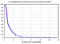
How to read the blue curve: find the point where AC voltage = 2.0V on the horizontal scale, and %Headphones = 15% on the vertical scale. This means: 15% of all headphones surveyed require 2.0V or more, to achieve 110dB SPL. It also means: 85% of all headphones surveyed require 2.0V or less, to achieve 110dB SPL
How to read the red curve: find the point where AC current = 30mA on the horizontal scale, and %Headphones = 17% on the vertical scale. This means: 17% of all headphones surveyed require 30mA or more, to achieve 110dB SPL. It also means: 83% of all headphones surveyed require 30mA or less, to achieve 110dB SPL
How to read the blue curve: find the point where AC voltage = 2.0V on the horizontal scale, and %Headphones = 15% on the vertical scale. This means: 15% of all headphones surveyed require 2.0V or more, to achieve 110dB SPL. It also means: 85% of all headphones surveyed require 2.0V or less, to achieve 110dB SPL
Attachments
Thanks, Mark. Good to know.10 ohms, 1.518v RMS 230 mW ---> 152 mA RMS , 215 mA peak30 ohms, 4.41v RMS 650 mW ---> 147 mA RMS , 208 mA peak50 ohms, 6.7v RMS 950 mW ---> 134 mA RMS , 190 mA peak
All of them are pretty much within experimental error of what you might expect to see, from an array of (follower + constant current load) cells, running at 203 mA idle current.
I will give a try to having J113 on top and bottom which I believe is how Mr. Pass designed one of his single-ended versions.
The PCB that I am using can be configured to bypass the cascode.
While I am waiting for PCBs to arrive for the series Micro Beast, I am re-visiting the complementary version. I am going to build a breadboard prototype of the circuit shown. The JFETs will be J113 and J175. One pile of J175 that I have has a group that is 24.x mA Idss @12v Vds. With a 100 ohm source resistor, the idle current is ~ 12mA. That makes power dissipation less than 1/2 of maximum.
I will match the J175 group with a similar Idss group of J113.
The potentiometer will be 200 ohms which should set proper idle current and allow making DC offset zero.
Drain resistors of the input JFETs are sized (hopefully) to allow voltage swing to drive the gain JFETs.
Voltage rails will be + / - 12v
This is intended to be a Stasis JFET Beast with a nod (two actually) to the master.
If this works, I want to scale up to a board size that achieves 1A idle current at + / - 12v rails.
Comments/criticisms/advice are welcomed.
Small update. I am characterizing JFETs to get some matched pairs.
The J175 require 100 ohms source resistance for 12 mA idle current.
The J113 require 50 ohms source resistance for 12 mA idle current.
The gain of the J175 is less than the gain of the J113.
gm of the J175 is ~10mS while the gm of the J113 is ~17 mS.
It looks like R3 and R4 can be adjusted to compensate for imbalance in gain between the N bank and the P bank.
That really looks like a micro version of F5 with a few add-ons.
Why did I think the original beast was a follower?
Why did I think the original beast was a follower?
For sure it looks like an F5. The inspiration is the attached NP Statsis OS from 1980/1990
No feedback but feed forward as Mr Pass has discussed in various threads

No feedback but feed forward as Mr Pass has discussed in various threads
The Stasis version is quite "fiddly" to sim with SPICE. I have tabled it for now.
I have made progress figuring out how to create a complementary version with JFETs that you can buy today in large-ish quantities at reasonable prices.
I have performed lots of measurements and created basic models that sim close to actual measurements of the JFETs.
A representative J113 has Idss of 21.x mA at 12v Vds and gm of 7 (all measured). The gm measurement is performed with an Rs that sets idle current to 1/2 of Idss; the way the JFET will be used in the basic cell.
A representative J176 has Idss of 11.x mA at 12v Vds and gm of 4 (all measured). The gm measurement is performed with an Rs that sets idle current to 1/2 of Idss; the way the JFET will be used in the basic cell.
While the J175 is a closer match to the J113 for Idss, the gm of the J175 by itself is 4 and is not a good complement to the J113.
If you parallel 2x of the J176, the Idss and gm are almost exactly that of the J113.
Attached is a sim of the basic cell that I will use for the next complementary mini/micro Beast.
The peak current is a little better than 2x of the idle current just before leaving class A. Again, its just a sim.
Interestingly, it looks like LTSPICE wants Vto (V pinch) to be measured at 1nA Ids. Not simple to perform for a lightly equipped DIY-er.
For anyone who wants to play along and/or contribute.....
In the spirit of playing along at home, I've been working on an SMD version of the Complementary Preamp/Driver:
Single sided board laid out (rear side is exposed copper to mount to a heatsink:
PCBWay did a fine job as always:
Laser cut stencil is a must:
341 hand mounted SMD parts later, ready to bake:
Forgot the turkey, baked a board instead!:
Board fired up...
No smoke, so that's a good sign.
The devices heat up a lot (expecting around 70°c rise above ambient based on datasheet curve).
Got 1.15A current draw on each +/-15V rail with their respective 64 devices.
DC offset is more than I'd like, but I didn't match the devices*
Bit of a waveform with input shorted:
20mV Pk-Pk, probably from not filtering the power enough**, or excess lead lengths during testing.
Ran out of time to play with this, but the board makes a sine wave at the output and no smoke, which is always a promising start!!
Thanks to Woofertester for continuing to work on these Beast variations.
* Aside 1:
I made a VGS Tester board based on Mark Johnson's schematic earlier in the thread.
I got part way through matching, but started having a few jfets fail, (TO-92 parts test fine still, so not sure what is going on.) so I decided to skip matching on the first board to get a baseline and revisit this when I get more time.
** Aside 2:
I did have a filter board to go between the SMPS and the boards.
Things happened and I experienced a large cap venting for the first time.
It was very exciting 😣
I am thrilled that you designed and built this SMT version. I know how much work went into it. Kudos.
I have a suggestion
Create a small PCB that you can use to measure Id. Have a source resistor in place on this board. The SMT version of the J175 has a max 225 mW dissipation. At 15v Vds, you want to limit current to 10mA for any individual device.
With 47 ohms Rs, I suspect some of your J175 devices are dissipating more than 225 mW. Maybe all of them.
For J113, I recommend between 70 and 80 ohms to keep Id at or below 10mA
In the picture attached, this J175 has Idss of 24.5mA at @12v and requires 150 ohms Rs to bring Id down to 10 mA.
The decade resistance PCB was acquired from Amazon.
I suggest that you make separate test PCBs for both J113 and J175. do not populate JFETs that cannot sustain close to 10mA with your chosen Rs.
Would you consider making a PCB version that is SMT for jfets and through hole for resistors? Then you could quantify each cell individually and populate a resistor individually suited to that jfet.
Thanks for your suggestions.
I had overlooked that the J175 had a lower max Pd than the J113. I took some measurements of a representative sample and found the J175s to be running in the region of 200mW - 240mW. For this board, I will try dropping the voltage to 9v or 12v and see how it goes.
Making a test jig to set the current could be feasible and then I could separate the devices with their matching resistors for population of the board.
It would be more complex than placing all the same value resistors and would require holding more resistor stock, but with proper organisation it wouldn't be too bad.
A hybrid approach is possible. The main challenge I set myself with this one was that I wanted it to be surface mount as much as possible with nothing on the rear side below the devices other than a ground plane that I could bond to a heatsink. I didn't include thermal vias on the board, which would improve the design, but that would be for another iteration depending how things go with this first one.
Attached is my current thinking for the single cell for the complementary Beast. This cell could be used to replicate the original Beast from Mr. Pass but using JFETs that are in production today. I am working on a simple layout that will be compatible with a simple double sided PCB. Two J176 JFETs in parallel are a decent complement to a single J113 both in Idss and in gm (gain).
The combined resistances to bring the cell to 10mA idle (R3 + R4 +Rpot) is about 150 ohms.
The drain resistors will allow assembling and adjusting each cell individually.
R3 and R4 can be adjusted as needed for different Idss JFETs
Perhaps add an separate resistor in the Q3 source? We can call it R4A. Should give some more room for differences between Q2 and Q3.
Good question. I sort out the differences. I will only place together in pairs JFETs with very closely matched Idss.
If you want to do mass placements with no effort expended on sorting and matching, then that would be someone else's gig.
My assertion is that if you want to do a large-ish Beast, you want pure JFET behavior, good balanced behavior etc. The effort for this kind of a build is
1. sorting/matching
2. populating
Just my viewpoint.......
I just received 1000 pcs of J176 that I am measuring and sorting. I already have 3000+ pcs of J113.
- Home
- Amplifiers
- Pass Labs
- Beast with 1000 JFETs redux?