I am very interested in this, is there an easy way to accommodate a hot source? Something putting out 3-5 Vrms? My 4 ohms speakers are quite sensitive and i mostly listen at low volumes, so i hardly need any (voltage) gain overall.
Hats off!To clarify what I built, the J175 is the P channel and J113 is the N channel. The J113 JFets have a 33 ohm source resistor installed. The J175 JFETs have a 47 ohm source resistor installed. The J175 requires a bit more throttling than the J113.
If you zoom in, you can see the 33 ohm and 47 ohm resistors.
View attachment 1374633
I like these ways, because only the do (it yourself), the practical experience takes us further.
But also my own experiences and verbalizations: Just three suggestions:
Are all these trannies on the same circuit? It's audible when they're not.
Unfortunately, the cross-sections of the components add up enormously, so that current and signal also diverge here.
The solder connections together form a really fat lump of solder.
I am very interested in this, is there an easy way to accommodate a hot source? Something putting out 3-5 Vrms? My 4 ohms speakers are quite sensitive and i mostly listen at low volumes, so i hardly need any (voltage) gain overall.
All of the Beasts are gain of 1 (slightly less) buffers. If you have a 5v RMS source, you make your power rails such that you can pass 5 v RMS without clipping; specifically + / - 15 rails should pass 5v RMS.

Can you talk a little about the Version 1 cascoded B1 follower/CCS boards?
cheers
I have an existing B1 80-cell PCB the same size as the complementary version. I am backtracking and making a small micro B1 that is cascode if the builder desires. I am trying different JFETs in the various positions in the circuit. So far, the J111, J112 and J113 seem to be the best choice for the current source and cascode positions. I am investigating which JFET to use in the gain position. I have a few candidates. Right now, new Micro Beast PCBs are in production for me to do some experiments. If this PCB works well, it can be a stand-alone preamp/driver and also possibly a headphone amp.
For the complementary 80-cell mini beast with 2 stages, all of the N JFET footprints are in parallel. Same for the P JFETs.Hats off!
I like these ways, because only the do (it yourself), the practical experience takes us further.
But also my own experiences and verbalizations: Just three suggestions:
Are all these trannies on the same circuit? It's audible when they're not.
Unfortunately, the cross-sections of the components add up enormously, so that current and signal also diverge here.
The solder connections together form a really fat lump of solder.
I am going to equivocate. The rails need to have the cascode voltage added. The V+ rail should be 21v to achieve a positive peak of 15v. The negative V- rail should be 16v for a a -15v negative swing. I will know more when I have a PCB populated and connected to some test equipment.All of the Beasts are gain of 1 (slightly less) buffers. If you have a 5v RMS source, you make your power rails such that you can pass 5 v RMS without clipping; specifically + / - 15 rails should pass 5v RMS.
Is this because the IDSS values differ between the J113 and the J175s you used? I noticed you said you didn't do any device matching.To clarify what I built, the J175 is the P channel and J113 is the N channel. The J113 JFets have a 33 ohm source resistor installed. The J175 JFETs have a 47 ohm source resistor installed. The J175 requires a bit more throttling than the J113.
So the Vgs(off) isn't a factor as much as the rails? I always thought it was important that the voltage swing present on the gate of the jfet receiving the signal should be so that it stays in the desired region. Leading me to guess a J111 would be preferable to a J113, for example. But i haven't looked at curves or plotted a load line yet.I am going to equivocate. The rails need to have the cascode voltage added. The V+ rail should be 21v to achieve a positive peak of 15v. The negative V- rail should be 16v for a a -15v negative swing. I will know more when I have a PCB populated and connected to some test equipment.
Example: both parallel, but different in circuit:For the complementary 80-cell mini beast with 2 stages, all of the N JFET footprints are in parallel. Same for the P JFETs.
Attachments
![DSCN0605[1].JPG](/community/data/attachments/1282/1282753-632fa8d7abb2fbb61a9f5d5dbb30360f.jpg?hash=EgKhLSeVKB)
Is this because the IDSS values differ between the J113 and the J175s you used? I noticed you said you didn't do any device matching.
Yes. I did Idss measurements on a large population and figured out how to match a pile of J113 to a pile of J175. Look back in this thread and you will see the spreadsheet that I created to evaluate the populations of JFETs.
I sorted the JFETs in to a pile that matched for Idss using the 33 and 47 ohm resistors. I created bins of what the Id was for that JFET with the 33 or 47 ohm resistor.
If you populate the PCB one cell at a time and measure Id and output voltage offset, you get a feel for compensating for output voltage offset by choosing the next pair mis-matched in opposite direction.
Mr Pass sorts his very large population for very close matches. I have a much smaller stash so I chose to create an overall balance by evaluating each cell and choosing the next cell to move the output voltage offset in a direction to make that offset closer to zero. With my method, I do not need a monstrously large stash.
If someone wants to use a different method for matching and populating, the PCB I designed will happily show the results of the different method.
For the new B1 version I am creating, there are three JFETs in each cell.So the Vgs(off) isn't a factor as much as the rails? I always thought it was important that the voltage swing present on the gate of the jfet receiving the signal should be so that it stays in the desired region. Leading me to guess a J111 would be preferable to a J113, for example. But i haven't looked at curves or plotted a load line yet.
1. current source JFET
2. current gain JFET
3. cascode Jfet
I am evaluating a low-noise high-gain JFET for the current gain position.
The new B1 PCB can also be populated for the simple single ended buffer cell. In that case I would use J113 in both positions since the J113 has twice the power handling of the J111
I am also working on a Vgs-off measurement rig.
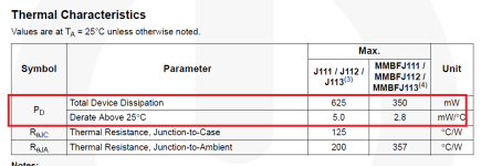
That will work for Vpinch matching. Unfortunately, 12 volts across a J113 with 1 ohm in the source may let out the magic smoke. I suggest 33 (minimum) to 47 ohms for that resistor.
For the above Vpinch setup, you do not know the drain current. I am working on a setup where you can set the pinch off current to what the datasheet test uses. The setup will use 2 DMMs. I am using very inexpensive DMMs so that my setup can be used by budget minded hobbyists.
For the above setup, the drain current is (Vpinch) / (1Meg // (DMM input impedance))
Do you know your DMM input impedance? Do you want to have to make this calculation over and over?
The text on the linked page does explain about the need to have a current limiter / series resistor in the power supply to retain the magic smoke.
Or to increase R1, but this also means dividing the DMM reading to read the current.
It also mentions that the meter will show a positive voltage, but seeing that the pinch-off voltage of a JFET is typically equal in magnitude but opposite in sign to VGS (off), you just have to put a '-' sign to your reading (also mentioned).
I'd be interested to see your design and how it works. I vaguely remember there was a thread of a design by Prasi some time ago also that I should try dig up.
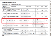
J113 Max IDSS = 25 mA . . . any higher and they'd ship it as a J111 , not a J113
With Vds = 12V and Ids = 0.025A the power dissipation is 0.3 watts, well within datasheet safety ratings. Zero danger of smoke emission. This continues to be true even when you hypothesize that somebody somewhere might someday receive a J113 with IDSS = 40 mA.
On the other hand, one very easy way to definitely release magic smoke, is to forward bias the gate-source or gate-drain PN junction and squirt a hundred milliamps through that teeny tiny diode. Which is why I (and Prasi's jig after me) install a 22 Kohm resistor in series with the device-under-test's gate electrode. This 22K resistor has no effect upon measured IDSS, but it sure saves your bacon when you install the D.U.T. rotated 180 degrees.
Attachments
Last edited:
Mark, I stand corrected. I was thinking of the J111.
I just checked a J111 and J113. The J113 was 27mA at 12 V
The J111 is going to be unhappy at 12v and a 1 ohm source resistor
I just checked a J111 and J113. The J113 was 27mA at 12 V
The J111 is going to be unhappy at 12v and a 1 ohm source resistor
I saw this one on Rod Elliott's site that I'm going to try out:
View attachment 1374936
Designing with JFETs
If you like this setup, use a Harbor Freight $7.00 multimeter and omit the 1 Meg resistor. The Harbor Freight multimeter has an input impedance of 1 Megohm. I just measured one of these multimeters.
The drain current will be Vpinch / 1 meg
I do not know what you are trying to convey with the two drawingsExample: both parallel, but different in circuit:
Are there any benefits in using the same device for all positions as the temperature drift is possibly similar?
Also it would enable/justify buying a larger number of devices from which to sort / match.
If using a single device do different roles require different sorting criteria? i.e. how would one choose where to put each device: Maybe pick devices with similar Idss for the gain position and just set the Id of the cell by varying the source resistance of the CCS?
I've seen cascodes used which reference the cascode gate to the gate of the `lower' gain device, or to the source of the `lower' gain device. I guess this results in the cascode device experiencing different bias voltage. Can you educate me on why you would choose either position?
- Home
- Amplifiers
- Pass Labs
- Beast with 1000 JFETs redux?