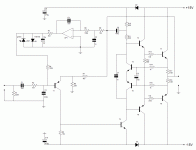
This is an amplifier I design, after studying many available designs.
Output stage complementary – darlington T3 – T6 –T7 – T8
Output bias current set with T4 – T5 ( mounted on heatsink )
Voltage gain T2 and bootstrap C6 – R10 – R11
Input & AC feedback T1 – R6 – R7
DC feedback OP1 – R4
Is there any hope for this design ?
Should I select transistors, recalculate everything and start building and testing ?
Attachments
T4-T5 are in a unstable configuration. They cannot address both sides at the same time; the emitters should be connected to the output too, but then C8 can cause havoc (blocking discharge when flipping of polarity occurs, not unusual when processing musical programs) and two resistors extra are needed to get things in control. Better stick to the classical solution to protect the output.
High value of R5 and T2 have to deal with everything, the poor chap. Ccb of T2 is going to reduce the bandwith considerable: unwanted phase deviation in the audiable spectrum. Instability is prone here.
High value of R5 and T2 have to deal with everything, the poor chap. Ccb of T2 is going to reduce the bandwith considerable: unwanted phase deviation in the audiable spectrum. Instability is prone here.
T4-T5 work to control the bias in the output stage. As long as the voltage across the output pair add up to 2Vbe(plus any voltage drop on the base resistors, which I would suggest could be reduced) this is a good way to bias Class A. Connecting the emitters to the centre rail will upset the bias arrangement.
I don't think the two bases need to be tied together with as large a capacitor as 33uF, probably 100nF OK.
I agree that 10k is too high. A lower resistor will improve things by allowing the PNP transistor current to increase, increasing the OLG and reducing distortion, and improve transient response. As the VAS is running at ~10mA the PNP should run at ~1mA, with changes in the CCS feeding it and about 680 ohms instead of 10k.
Last edited:
As soon as the stable dc operation is changed by modulation from an ac source, in what way is guaranteed that this 2Vbe+~ is unchanged? Depending on sourcing or sinking current to the load, the Vbe's of T7 and T8 do change and not in equal amount.
Suppose T7 is near switching of (Vbe < 0.2V), how is determined that Vbe of T8 is 1.8V? By the current through the load? Mayby T8 is at not yet at that value with the demanded current, but only at, say, 1.5V. Total bias is now reduced to 1.8V. T4 has switched off already and no bias control anymore.
Or can be assumed that T4 and T5 will stick T3-T6-T7-T8 at a total of '2Vbe' unconditionally? But how? What is controlling the behaviour of T4-T5? The voltage over R17-R18 is depending on the demanded current through the load and the exponential curves of T3-T6-T7-T8. They don't make an agreement to stay awake all the time.
T4-T5 are not a bias voltage source as intended. There is no bias control. Build it.
Have you actually simulated this?
As long as the current through T4-T5 is approximately constant, the Vbe's will be as constant accordingly. With driver transistors and output devices taking reasonably low currents, the two transistors will keep the average current through the output pair more or less constant. So if T7 conducts more, T8 will be forced to conduct less.
Think it through again.
Last edited:
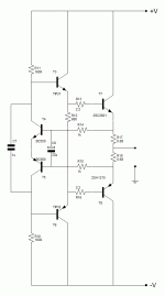
Ultra-low Distortion Class-A Amplifier
sound-au.com
sound-au.com
An externally hosted image should be here but it was not working when we last tested it.
Well, that circuit would have used the original RCA2N3055 (now H and now pretty much unobtanium). It would benefit from modern devices, giving a higher bandwidth, and could use a complementary output stage. That would be able to utilise the complementary bias circuit suggested by the OP, which works to D.C. and does not require a large filter capacitor.
The input stage transistor operates at somewhat low current. Perhaps around 40uA base current and 60uA in the 10k resistor which as discussed above is too high for a good frequency response.
Therefore, this design could well have very low distortion for a 1kHz test signal but the input stage is prone to being cut off (transient intermodulation distortion) in fast transients.
The BC107 Vas transistor operates at around 5mA. Its input impedance will be around 1k, so the base resistor could be 1k without too much difficulty, increasing the input stage current to 600uA. The loss of OLG can be offset by reducing the feedback resistor/grounding resistor.
I would not implement these changes without simulating and checking stability as the old 3055's often provided enough gain roll-off to provide the stability needed which these mods would override. Compensation capacitors are almost certainly going to be required, and I would strongly recommend Bailey's inclusive approach rather than a Miller.
While I would recommend this option as an AC coupled design the output capacitor should be a lot larger for good bass response (10mF).
Some points - the lower half of the output stage is somewhat voltage limited by the diode in the power supply and saturation of the VAS transistor. In a quick simulation, negative clipping occurs at around 12V while positive clipping doesnt. I'd suggest removing the diode, and even adding the double bootstrap Mullard once used in one of their amps.
To do this, the current values of the upper bootstrap resistors are replicated in the lower half, while the upper bootstraps themselves are halved in value. The VAS is re-routed so the collector connects to the upper driver base, not the lower one. The new bootstrap cap to the reduced resistors should be double the original (an extra 220uF cap if the 100uF is routed to the lower bootstrap now).
Using the lower bias resistors (680 ohm base resistor, 6820 ohm feedback resistor and 68 ohm grounding resistor) for the input stage may need a 220pF-100 ohm series RC pair connected between the collector of the VAS and emitter of the PNP input for stability.
If the bias transistor base resistors are reduced to 220 ohm , you will need 1uF caps across the bases, higher than I originally said, to reduce possibility of oscillations.
I have not used DC servos, and I note that yours has a nasty peak at around 1Hz. As a rule, I try to avoid lots of LF time constants, and you have 3 which is potentially unstable.
It's probably OK if you have a strictly LF limited preamp, but I try to play safe. If I were to use a servo I'd use a single time constant (e.g. 1M-1uF around the opamp) (or at the most 2) and a small capacitor only on the output feeding the base resistor just to minimise HF feedthrough. Reducing the input cap to 1uF limits the bass response a little, but eliminates the peak.
The only other concern I have is that you may find there is a turn-on thump as the various capacitor(s) in the servo get to their operating voltage, because the base has to sit at ~-.6V or so which has to charge through the input capacitor as well. this may be fixed with either an output delayed relay or rise-time limited power supply. Haven't looked into that. I've only known completely thump-free amps where it was fully D.C. coupled with differential FET input (very low I/P offset voltage and zero once trimmed) or A.C. coupled where both sides are identical (eg. in a classic design with 470 ohm feedback "grounding" resistor and 1mF decoupling cap, the input is also fed through 1mF and 470 ohms (which can double as an RF filter), and the intermediate stages are symmetrical too.
Last edited:
I've done some calculations on dc-stable operation (no input signal), and it seems ok for now. But modulating this balance is what counts: does it hold up during dc variations mimicing the ac response? I'm going to simulate this dynamic dc stability - it is not working (my expectation), or the nasty class AB problem has been solved finally with this bias circuit!T4-T5 work to control the bias in the output stage. As long as the voltage across the output pair add up to 2Vbe(plus any voltage drop on the base resistors, which I would suggest could be reduced) this is a good way to bias Class A. Connecting the emitters to the centre rail will upset the bias arrangement.
When T1 is running 1mA, the servo will force it to -5.3Vdc at the base (calculatation through R7); led1 is very hot then. Those circuits demands very low currents in the input stage (no differential).I agree that 10k is too high. A lower resistor will improve things by allowing the PNP transistor current to increase, increasing the OLG and reducing distortion, and improve transient response. As the VAS is running at ~10mA the PNP should run at ~1mA, with changes in the CCS feeding it and about 680 ohms instead of 10k.
Yes, I would not recommend changing the input stage bias without changing the servo circuit. I did not use the LED and diode in my simulation. You could also change the 100k for 10k and input capacitor to 10u for example.
But it's up to the designer to set the current, it's not "the circuit demanding it".
The VAS runs at about 15mA, which makes the input impedance to the VAS around 200 ohms or so. A higher input stage current requires a lower base-emitter resistance, so 680 ohms is not going to reduce the gain by more than about 30%. More than that can be regained with a lower feedback network impedance, which gives lower distortion.
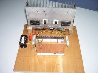
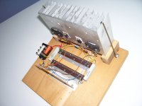
I had some spare time this week and I build a power supply, and fit 4 transistors on a heatsink, soon I will make some test.
About C3 330n .. should be 33p ...typo error.
Current in VAS: 1640 ohms resistance, 15 volts supply voltage and a few junction I expect around 7.5 mA.
T1 with current too low and too close to cutoff I agree I will have to modify this one.
If current in T1 reach 1 mA , voltage across R6 will be around 220mV and voltage at the base of T1 will be around -1 volt. Diode D1 and green led are some kind of protection to limit voltage at the base of T1 and keep output voltage close to zero even in the worst case. ( servo faillure )
Using boostrap on upper and lower side is a new idea for me, I will think about it, it would give more voltage swing on lower side.
I f I understand, upper boostrap resistors should be 390 ohms and on this side current is 16 mA, on the lower side resistors should be 820 ohms an current on this side is still 7.5mA, and transistor T2 connected to the base of T3 pick up the difference.
I will start testing soon and see if output bias works as expected.
Thank to everybody
Your input T1 is similar to JLH 1969. It uses at Ic 200ua and every body is happy with. Ksa992 low current transistor is best suited. In sublimed JLH1969 I increased the current by current mirror, but LM334 can also be used.
I made a first test, with rail to rail voltage from 15 volts to 37 volts bias current drifted of about 7% from 1.00 amp to 1.07 amp.
Then I left the unit heat by himself until sink temperature rise fron 20 deg C to 41 de C the bias current did not change.
But i noticed some noise on V+ and V- rail ( noise from rectifiers at the end of condution ) this noise spread everywhere in the unit. I am affraid I will have to neutralise rectifiers noise with capacitors installed very close to the rectifier.
I am using a very heavy bridge (KBPC 25-04) 25 amp 400 volts. If I change to something smaller with less junction capacitance should I expect to have less noise ? Or use faster Schottky rectifiers ?
It is recommended to mount smoothing capacitors as close to the rectifiers as possible. Regarding the "noise", is this mains-frequency related? Your test circuit is OK except there is no filtering on the bias chain, so power supply ripple will get into the bias.
If you decouple the bias chain with small resistors and large-ish capacitors that should solve the problem.
Another option would be to put a capacitor on one of the collectors of the bias transistors (as a sort of input connection) and ground that to quieten the ripple.
If it is other noise, then that requires a different solution.
I did get rid of oscillations, something I should have made in the first time: adding decoupling capacitors on supply rails.
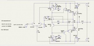
Here is what I have now with measured voltage.
25 mV offset for a rig of this kind is something you see only once in your life, but it is there.
Next step will be to ad boostrasp and after that voltage gain+ AC feedback
Here is what I have now with measured voltage.
25 mV offset for a rig of this kind is something you see only once in your life, but it is there.
Next step will be to ad boostrasp and after that voltage gain+ AC feedback
Attachments
- Home
- Amplifiers
- Solid State
- basic class A