I put boostrap to work ... it did ..so now R11 is working as a current source, so current through R101 connected to negative supply rail have a constant current and PSRR has drop.
Before 2 resistors made a voltage divider betwen positive rail and negative rail since ripple is symetric on both side it neutalise each other.
Now output signal is as noisy as negative rail.
The only solution I can see is to get rid of the ripple on negative rail.
Otherwise this noise will have to be erased by the action of the feedback circuit.
Is there any known solution for this situation?
Attachments
The noise on the output from the negative rail is induced through T6 and T8, whereas before the addition of C6 this also happened from the positive rail through T3 and T7, but of (almost) opposite phase cancelling most noise--ripple out. Adding another bootstrap Cx (splitting R101 in two equal values) should recancel the noise.
When putting a signal driving transistor at that place (T2 in the original), on both positive side (bootstrap cap) and negative side (T2) signal and noise are present, but the signal remaining (both in same phase) while noise is rejected (opposite phase), resulting to the same (hopefully enough) silent output. That's why often the combo R5-T2 is made with a current mirror to reduce ripple-leakage through T2 even further.
When putting a signal driving transistor at that place (T2 in the original), on both positive side (bootstrap cap) and negative side (T2) signal and noise are present, but the signal remaining (both in same phase) while noise is rejected (opposite phase), resulting to the same (hopefully enough) silent output. That's why often the combo R5-T2 is made with a current mirror to reduce ripple-leakage through T2 even further.
A bigger C10 and resistor to filter the negative rail would work, if, and I should have mentioned, a similar filter was used on the positive rail.
When dealing with balanced circuits, balance needs to be maintained on each half. I agree, a bootstrap should also have been added to the lower half.
My original suggestion to add input capacitor (or two) and ground the input would also have worked.
When dealing with balanced circuits, balance needs to be maintained on each half. I agree, a bootstrap should also have been added to the lower half.
My original suggestion to add input capacitor (or two) and ground the input would also have worked.
... decoupling the bias resistors will also give a quieter output than double bootstrapping.
Bootstrapping the lower half only gets you to the ripple voltage that you had originally.
Filtering actually reduces the magnitude.
So indeed, a bigger C10 but also add one in the positive side.
Bootstrapping the lower half only gets you to the ripple voltage that you had originally.
Filtering actually reduces the magnitude.
So indeed, a bigger C10 but also add one in the positive side.
Bootstrapping the lower half only gets you to the ripple voltage that you had originally. Filtering actually reduces the magnitude.
It's the way of regarding such a circuit and where noise (power ripple) originates from if one side is bootstrapped. Indeed the initial state of noise is again reached, whereas reduction is reached with better suppression of noise at the source (in this situation the power rails).
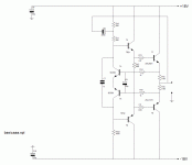
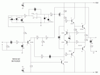
I made few more test....gain is indeed very high and circuit oscillate.
But gain can be reduced if the current in the feedack voltage divider is changed, I use the circuit you see below, and I change resistor '' TEST R '' if value is above 360 ohms there is no oscillation, if the resistor is below 360 gain get high an I get oscillations.
Using 470 ohms circuit is stable without any compensation ( no signal ). I will make more elaborate testing soon.
In the circuit as shown the feedback is a '' Y '' configuration, easier to modify for testing but any time it can be transform to a simple equivalent voltage divider.
Attachments
The frequency response is likely to be limited by the internal collector-base capacitance of T2, coupled with "Test R" (plus equivalent of the feedback pair) but also the TIP31/32 as drivers is not an ideal choice as these are slow (around 3 MHz). The circuit will probably be better with BD139/BD140 and rather than having base resistors in the output pair, base resistors in series with these drivers (about 100 ohms) should suffice.
I would also suggest that a phase lead compensation capacitor (connected between T2 collector and T1 emitter) would help to stabilise the gain with lower "Test R". That may require a series limiting resistor too to correct a spike at very high frequencies.
JLH much preferred this compensation method, as did Bailey, and it worked well for them rather than Miller. It works when there are only two transistors in the loop, as here, but with higher gain (Darlington T2, or equivalent) that keeps the gain high while the phase delays increase, making Miller the standard approach for such designs.
OK, I took up the challenge. Here is a simulation of almost your circuit with my proposed transistor line up and compensation.
The audio signal is a 100mV (peak) 5kHz one while the amplifier is also fed with a 50 kHz square wave of 900mV (peak to peak 1.8V).
There is no visible glitch due to transient intermodulation distortion in the recovered signal (upper graph) while the lower graph shows the actual output. (red graph)
Miller designs can fail this test.
THD in the recovered signal is 0.2%, and the amp is working near max output.
Attachments

Last edited:
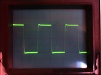
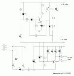
Made a lot of progres today, ad a ZOBEL at output, ZOBEL did kill oscillation even with no compensation. Then test with signal and load, and add some compensation. Here is the result with 20 ohms resistive load, ZOBEL at output and compensation 220 ohms + 47pf. Signal is 50KhZ square wave and output 20 volts peak to peak.
Attachments
It's clear my thoughts in #3 and #5 prove wrong: hurray! In #12 I follow this track onwards. In #31 a nice tempered square @ 50kHz... the front stepstone indicate fast but not overly slewing. I'm about to buy a hat... to take it off for this!
I am still working on my spare time.
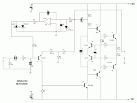
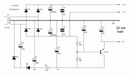
I am using a simple power supply for testing , a pair of 48000 uF capacitor and a bridge rectifier. In the final amplifier I do no expect to have huge capacitors and it will have 2 chanel. So power supply noise will increase and I noticed that a fair part of ouput noise come from negative rail of power supply through T1 & T2.
So I desing a special supply for this part of the circuit: a voltage doubler plus a ripple filter. Thi way I will reduce power supply noise for T1 T2 and it will also increase voltage for T2.
I expect this modification to make T2 more linear since it will have around 4 more volts collector emitter and will not have to go to saturation or close to saturation for maximum output.
Attachments
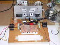
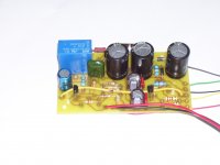
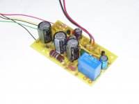
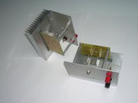
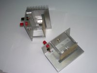
Now I have a delay circuit for turn-on thump, and I have PCB, delay & bias are made and tested, also a fair part of hardware made. Some component value have been change since I try to use components I have at home.
Feel free to comment, I always read comment and I have learned a lot, thank you.
Feel free to comment, I always read comment and I have learned a lot, thank you.
Attachments
- Home
- Amplifiers
- Solid State
- basic class A