No ! no insulators are needed as you see in this PDF the mounting base is already isolated.
http://www.ixys.net/Documents/AppNotes/IXAN0073.pdf
http://www.ixys.net/Documents/AppNotes/IXAN0073.pdf
well , maybe it's a fact that English is not my native language ...... but at least I can't follow you there ;
what offset you're mentioning , when simple current tests are in question?
again - brake circuit in two halves , test exactly per this two schematics , put A -meter where appropriate , and put gate resistors ditto at mosfets if you already didn't
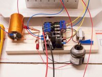
I have now done the first test - the lower part of the circuit - as suggested by ZM following his illustrated schematic 100%.
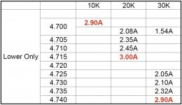
After spending more than 8 hours allowing the heat sink temperature to reach relative equilibrium, around 130°, and doing multiple runs to repeat the findings, the device simply cannot be biased to 3A2 at +30V - the current draw starts to runaway at around 2A9, regardless of which voltage was applied to get it there. Below 2A9, the dv/di is not predictably linear. It behaved exactly like a switching device - please see attached picture.
At this point I will pause on this project and await others with more knowledge and experience to make it work, and I am happy to follow. Thanks to everyone who helped and guided this along, this is now well beyond my abilities.
Attachments
well done ci11…..clear experimental result….there seems to be a problem.
Same device next gladiator, please…..
😀😀
Same device next gladiator, please…..
😀😀
ci11
I admire your patience and dedication - I will try to p to p the circuit together with my parts over the next week . This is not to say that I think you missed anything but just using my parts.
Best
Bob
I admire your patience and dedication - I will try to p to p the circuit together with my parts over the next week . This is not to say that I think you missed anything but just using my parts.
Best
Bob
After spending more than 8 hours allowing the heat sink temperature to reach relative equilibrium, around 130°, and doing multiple runs to repeat the findings, the device simply cannot be biased to 3A2 at +30V - the current draw starts to runaway at around 2A9, regardless of which voltage was applied to get it there.
.
Repeat with 25V supply.
P.S. Just for confirmation is that 130 F or 130 C?

Don't forget this is very much a thermal problem as it is a current problem.
Probably still thermally run away but he might be lucky.
Probably still thermally run away but he might be lucky.
If that fails put two 0.22 ohm resistors in parallel (0.11 Ohms source resistance) at source pin of bottom mosfet that should be adequate to stop it thermally running away.
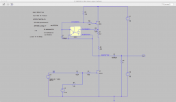
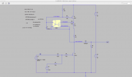
I occupied a bit more with the BAF2015 II circuit…… 🙂
I found that Microsemi offers the Spice models for their linear Power Mosfets on their site.
So I got the .lib for an APL502J and because I am bad with Spice I asked Zen Mod to implement the .lib in my Spice. That is such a pleasure, short time later I got the working Spice….. 🙂
As you can see I tried the APL at the moment without the Jensen, only to see if the circuit works without the Jump in current ci11 showed here.
And it worked….
but the bias voltage must be carefully adjusted, even 0.01V make with these parts a difference.
I know that ci11 could adjust his bench supply in finest steps, so it is still open why his experiment showed the current flash.
Keep in mind, no feedback, horrible gain so…..
I will show with some pictures what happens with the APL part with small voltage changes…..
Attachments

Last edited:
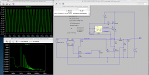
and here two pictures that show how tiny changes in bias voltage make big effects.
first picture V bias = 3.49 and voltage out the output node 42.67V
second picture Vbias = 3.58V and voltage at the output node 607mV
Ha, Ha no easy circuit even for simulating gladiators…..🙂
first picture V bias = 3.49 and voltage out the output node 42.67V
second picture Vbias = 3.58V and voltage at the output node 607mV
Ha, Ha no easy circuit even for simulating gladiators…..🙂
Attachments
- Status
- Not open for further replies.
- Home
- Amplifiers
- Pass Labs
- BAF 2015 Coverage