Hehe, guess you did. Cleaner power at the bias boards/OS. I will try it using the headphone trick, might not be an issue with loop at all.
@6L6, I noticed that the 22R0 resistors on the Front End Board are raised and appear to be of higher wattage. In the Bill of Materials they are listed as 1/4 watt.
I'm currently working on the F6 with the TM 5U Chassis, but some wiring parts are still on the road. So I have time on my hands. The BA3 will go in the second TM chassis.
I'm currently working on the F6 with the TM 5U Chassis, but some wiring parts are still on the road. So I have time on my hands. The BA3 will go in the second TM chassis.
Are these good for ba-2 output stage?
I don't see why not. The FQA12P20 in particular should not have the
transconductance issue mentioned in the BA2 article, and was the P channel
part used in the F5.
The only thing I would caution is that these parts have been discontinued for
a number years (probably a decade) so I would be concerned about
counterfeits unless they are of known provenance.

Thanks, guys! Really appreciate it.
ZM: I’ll post some more once I am proper happy. Too much of a mess in there right now to let you hammer it.
But regarding the Porn bit, my fat can cap & choke plans are not yet realized so no joy there, nor porn nor iron. I can take a picture of it’s rear end and post it, but I must warn you, the inputs are pretty standard.
😀
Front End Gain Increase
Dear All hi,
Is it ok if we increase the value of R13 (330 ohm) to 390 ohm at the Front End in order to get more gain and have more “head room” at low levels listening in my set up conditions (not so sensitive speakers (82 db at 1 watt at 1 meter)) or we are going to get in to trouble.
Gain calculation according to nelson’s instructions is R13/R10 (330 ohm/22 ohm=15 db) a total of around 30 db.
If we increase R13 to 390 ohm we get (390 ohm/22 ohm=17,72 db) a total of around 35,44 db.
Thanks
I've been tweaking my existing BA-3 to move along the journey I'd started. From previous posts, I built a "standard" BA-3 with 6 devices per side and 24V rails. I experimented a while with different output bias settings to try and learn. I also wanted to see how far I could push the heatsinks comfortably.
I got a new 4U/500 chassis (thanks 2 Pico Dumbs and Gianluca). So, it was ideally suited for trying the "original" 12 device per side complimentary output stage.
I've got all that in and working. I'm very happy. Now onto a few questions as I continue to learn
As many have noticed, the BA-3 front end bias and offset can be fairly "touchy". It is relatively temperature sensitive. In my case, just removing the cover for a brief measurement causes it to move so much that it's hard to "center it" around a value. I'm not terribly concerned, but I'd love to know if there's a way to make it a bit more temperature stable.
I noticed in Papa's article, it states "R8 and R9 help set the voltage gain, and they also help stabilize the bias of Q3 and Q4, else it would tend to drift upwards as the parts warm up."
Those resistors also play a part per the article toward setting the overall bias along with R13.
Has anyone altered the values of R8/R9 toward the goal of a bit more temperature stability? Can you share your observations?
I am also ordering some larger sinks for Q3/Q4. Mine are too wimpy, I believe, and that could contribute to the wandering. A bit more mass to help keep temps stable would be great.
Thanks in advance for any insights!
mess, obviously, or I'm even shorter brain-wise than usual 
see my post from 18th sept.2011 on this page: Burning Amplifier BA-3 - Page 2 - diyAudio
there I tried to rectify Papa's mess with nomenclatue (h proably wrote by one, while posted article with later schm)
pic thumbnails ain article are empty, but schematic is here at click...... anyway - here it is
you're asking, in fact, about R10 and R11 - source resistors; they're doing exactly that - decreasing all temp. induced changes, by degeneration
increase them, to make mosfets more behave, but in that case - to keep Iq of mosfets same, you must dial up JFet drain resistances
see my post from 18th sept.2011 on this page: Burning Amplifier BA-3 - Page 2 - diyAudio
there I tried to rectify Papa's mess with nomenclatue (h proably wrote by one, while posted article with later schm)
oooooh Greedy Lazy Boyz
Papa must do all hard work for ya .....
here it is - nomenclature by schmtc :
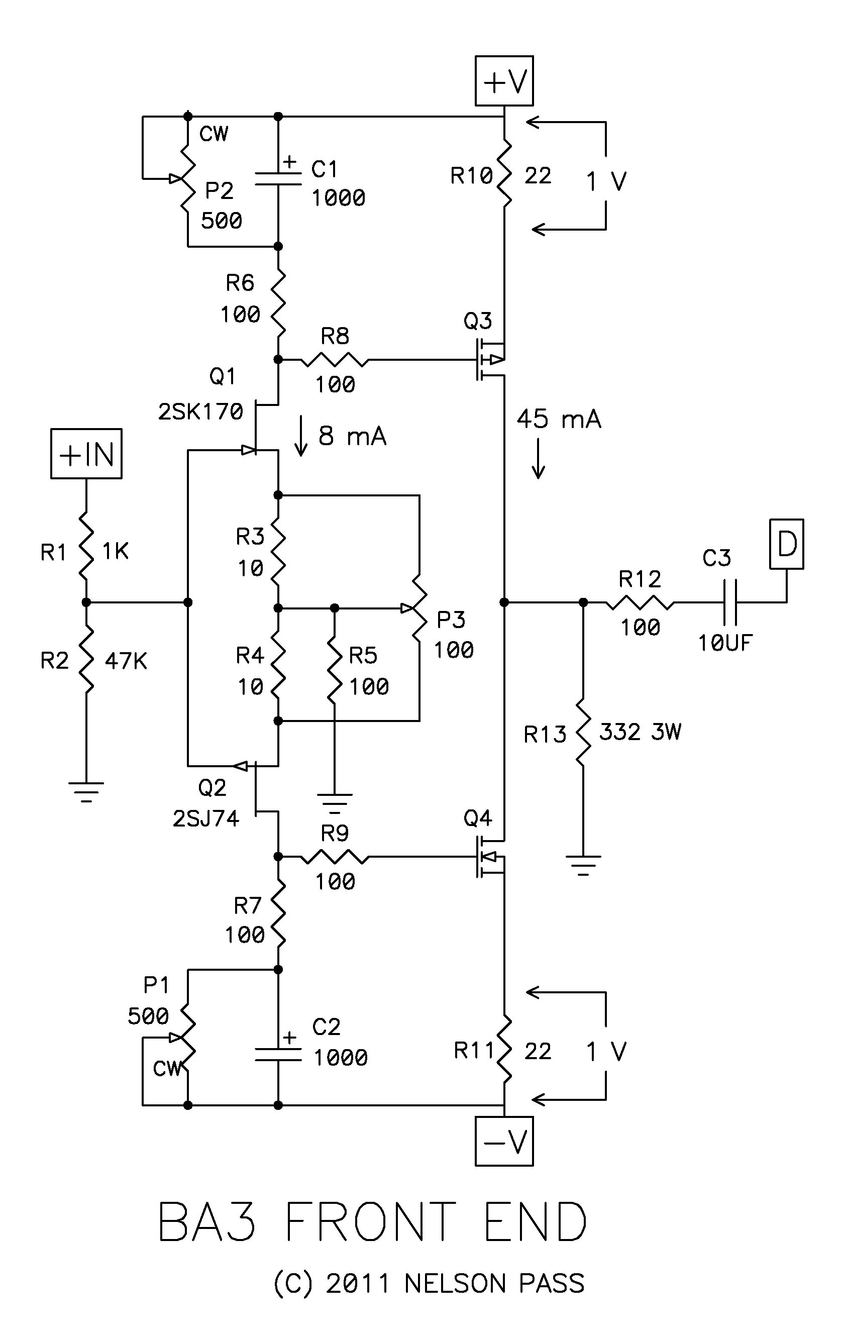
" This is familiar enough. Q1 and Q2 are JFETs which self-bias into resistors R3 and R4 at currents around 8 mA. R1 is chosen to avoid oscillatory interaction with whatever source impedance you might have, and R2 provides a DC reference to ground in the event that the source does not, and also establishes the nominal input impedance.
Q1 and Q2 are largely degenerated by R5, setting the amount of AC current which flows through them for a given input voltage. The voltage gain of this initial stage is approximately
the value of Drain load resistors R6 plus R7 divided by R5. In this case we have roughly unity gain – the Jfets are used as unity gain DC level shifters to Q3 and Q4.
Coming off the Drain of Q1 is the loading network of R6, C1 and P2, and there is a comparable network of R7, C2, and P1 attached to the Drain of Q2. R6 clearly sets the AC load for Q1, but the DC requirements to bias up Mosfet Q3 are higher than that, so P2 in parallel with C1 provides a higher resistance value below about 0.5 Hz, and gives the approximately 3 volt DC drop required to bias the Mosfets.
P1 and P2 are adjusted so as to set the DC bias of Q3 and Q4. You will want to set them at zero when you first fire up the circuit, and increase their resistance to achieve the correct bias voltages across R10 and R11 (about 1 volt) while also keeping the output DC offset voltage at a minimum. This circuit is capacitively coupled at the output, but low offset measured at the Drains of Q3 and Q4 will maximize your output voltage swing.
The voltage appearing at the Gate of Q3 is amplified by something less than the ratio of R13 divided by R10, and with the same happening at Q4(R11) and considering the transconductance of the Mosfets, comes out at about 15. Both of them added make a system voltage gain of about 30X, or 30 dB.
R10 and R11 help set the voltage gain, and they also help stabilize the bias of Q3 and Q4, else it would tend to drift upwards as the parts warm up. The bias current here is about 50 mA, and it will deliver peaks of approximately 100 mA. Q3 and Q4 require heat sinks.
Of course you can bias this circuit higher if you wish – 100 mA bias is perfectly OK as long as you properly heat sink Q3 and Q4, and if you are crazy (like me) you can experiment with higher bias, remembering that the parts are rated at 25 watts, and that it costs you voltage losses across R10 and R11. If you want to play with even higher bias, you can consider lowering the values of R10 and R11 and also R13, all in proportion.
The supply voltage is only critical with respect to the voltage rating of the input JFETs, which are nominally 25 volts. In actual testing, they break down around 40 volts. I wouldn't worry about running them as high as 30V. Hot-rodding this circuit would likely involve cascoding the input Jfets to allow higher voltages. "
pic thumbnails ain article are empty, but schematic is here at click...... anyway - here it is
you're asking, in fact, about R10 and R11 - source resistors; they're doing exactly that - decreasing all temp. induced changes, by degeneration
increase them, to make mosfets more behave, but in that case - to keep Iq of mosfets same, you must dial up JFet drain resistances
Yes, but at the expense of more voltage drops across them.
I have achieved some success in stabilizing this unstable IQ/offset by putting all three meters where they should be, and putting the lid on.
Then waiting 1-2 hours until it all settles real nice, equilibrium and all that.
Then adjusting, putting on lid. Waaaaait
Readjusting, putting on lid, waaaait
Readjusting, putting on lid.
I usually spend two hours each time. But doing this with lid on and amp in it’s seat in the listening room, get’s stable values over time. I am slow, I know, but get’s there everytime.
Adjusting with lid off does not work, offset will be off anything from 100-250mv once up to temp with lid on.
I don’t think I would increase R10 and 11. If you get more sink, I would probably try less degen and more bias, papa style. Have been considering it.
I got offset pretty stable with 65ma bias with small sinks. But stable is relative... plus minus 15-30mv is the best I have achieved at those temps/levels. But a cats fart in the room will affect the drift, so...
A tip: if you spend the same amount of time adjusting offset each time, meaning lid off for equal amount of seconds, you can pretty much predict the offset drift with lid off. In my case, at equilibrium, the drift is approx 30mv on the pos side. So with lid open for approx 10 sec, I adjust offset to +30mv, then put lid on, then see how it goes after a few minutes or many (stabilize). It often ends up around 0, but some drift there will always be.
Zen Mod: with your finger in the air waiting for the warm breeze to come from some direction, how much offset will affect distortion levels audibly? I too need to know this for future P3 adjustments.
Drift will affect voltage swing, but I would not worry about +/-50mv, though I always target 0 +/- 10-15mv.
Physically isolating the front end might help, and using a case with minimal ventilation/air flow across jfets.
I should think sinking the JFETs would provide much more stability than the adverse effects of increasing MOSFET source resistance. A BIG sink on your MOSFETs will probably work wonders too.
I would LOVE to see a pic of the 6 deep config, as I have considered it myself. How does it sound compared to 3 deep?
I really enjoy seeing and reading about your builds, it is inspiring and you take it all to the next level. Really cool! Those notes of yours too might soon be worth a pretty penny.
Andy
Last edited:
remember that there is a cap in between FE and OS
so, whatever FE is drifting, it has nothing with OS drift - neither Iq, nor DC offset
build it, route probes of zillion DMMs outa box, put lid on from moment when you at 80% of setting procedure and continue as that - pull off, twidledee to half, put on, wait, repeat
you want more stable?
devise or plead either for NFB or for servo(s)
Plead for NFB? I at least resent the thought.
I think the BA-3 was built to drift, hence the output cap. But always nice to have it nice and low.
I plead for bias, much bias. Big FE MOSFET heatsinks, less source resistance, 100ma bias, and maybe some specially home made greedy boyz ZM JFET heatsinks, and happy times.
I think the BA-3 was built to drift, hence the output cap. But always nice to have it nice and low.
I plead for bias, much bias. Big FE MOSFET heatsinks, less source resistance, 100ma bias, and maybe some specially home made greedy boyz ZM JFET heatsinks, and happy times.
Last edited:
From papas article:
«You can also vary the bias current of Q1 and Q2. You measure the current by reading the voltage across R3 or R4. With 10 ohm, the voltage wants to be 0.08 volts for 8 mA of current. You can play with this, but keep in mind that the dissipation of this part is rated at 400 mW, and for this circuit 10 mA will represent around 200 mW. These JFETs were chosen at Idss figures of 10 mA (Idss is the current that flows when the Gate and Source are at the same voltage). If you get lower values, you may want to consider higher values for P1 and P2, say 1 Kohm. They are best matched, but P3 can be adjusted to compensate for some mismatch.»
I measure around 55-60mv drop across R3 and R4 when set to same voltsge drop level. That equates to 5-6ma current, 2-3ma below spec. I guess this is due to lower IDSS values?
I wonder how this affects sound, and if I should change values of R3 and 4 for final iteration iot bring the JFETs up to 8ma.
Any takers and thoughts?
Cheers,
Andy
- Home
- Amplifiers
- Pass Labs
- BA-3 Amplifier illustrated build guide