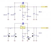
mind the different pins of the regulators...
I suggest we go better to PM communication because we are a bit away from B1....... O.K.?
I suggest we go better to PM communication because we are a bit away from B1....... O.K.?
Simply use 317/337 for alternative or adjustable, regulated voltages.
The 79xx and 78xx series were designed for fixed regulated voltages.
The 79xx and 78xx series were designed for fixed regulated voltages.
The minimum Vdrop (drop out) of the 78/79 and the 317/337 are similar.
Maybe you need to look at LDO (Low voltage Drop Output) regulators. But, be careful, they are not as tolerant of component guessing.
Maybe you need to look at LDO (Low voltage Drop Output) regulators. But, be careful, they are not as tolerant of component guessing.
Output Caps
Since my Amp already has a Input cap (4.7uf) do I you really need C101,102 if the only function of C101 & C201 is to form a high pass output filter and block DC passing to the next stage ? Any other reason to keep them in the circuit if your amp is ac coupled this for the standard b1 build.
Since my Amp already has a Input cap (4.7uf) do I you really need C101,102 if the only function of C101 & C201 is to form a high pass output filter and block DC passing to the next stage ? Any other reason to keep them in the circuit if your amp is ac coupled this for the standard b1 build.
Where DC exists or can develop during a fault condition and it is required that that DC voltage be blocked from passing to the next stage, then one needs only 1 DC blocker at that link.
The DC blocker can be located at the output of the source equipment
or
at the input to the receiving stage.
One does not need to block the DC twice.
The user needs reassurance that when he/she connects A to B that there is no to little risk of damage.
the easy way for manufacturers is to always fit a DC blocker at the output of all their equipment and for those same manufacturers always to fit a DC blocker at the input of their equipment.
If you the builder decides to take on the design role, then you need to reassure the user/s that you have designed the equipment such that it does not damage it's self.
How do you do that?
I have my solutions.
What are yours?
1st. I started another thread and should have used this one. This thread is unreal! So much information!
I'm interested in building a B1 Buffer and using the PCB.
I'd build the buffer and not use the source 1 / 2 select. This would be pretty simple with just 2 jumpers in the PCB to force the PCB to only use the input 1.
The volume piece I'm not sure what I'd do to bypass the volume pot/attenuator.
Each channel on the PCB for the Pot/Attenuator has a "CCW", "W" and "CW" to connect to the Pot/Attenuator. I'm guessing a jumper introduced to this area would pass the signal in full. I want a pure buffer without attenuation.
I appreciate any help!!
Mantha - Bypassing the selector is easy, just solder 2 jumpers in the middle of the board. Bypassing the Volume will be similar, I think you would just jumper CW to W. A simple continuity test would verify.
Last edited:
PS - The B1 buffer will not add any gain to the signal if I'm not mistaken if I build with Nelson Pass's specs... Correct? I'm 99% sure that is the case. That is what I want really..
I think I just exposed my inexperience with all of this by asking..
I think I just exposed my inexperience with all of this by asking..
Yes, the B1 has no gain. (+0dB or 1times)
The maximum output from your Source is passed through to become the maximum input to your Receiver.
If you bypass the selector and also bypass the volume control, you are left with so little, that you don't need a PCB.
The maximum output from your Source is passed through to become the maximum input to your Receiver.
If you bypass the selector and also bypass the volume control, you are left with so little, that you don't need a PCB.
If you look towards the beginning of the builds, a lot of them were like Andrew describes and truthfully its a simply thing to do. Perfboard might be the easiest route to make sure you never get a short but wiring in the air is still easy with this circuit., you are left with so little, that you don't need a PCB.
Sure,
I'm thinking perfboard. I wonder if I can just buy the JFET s matched from the pass site... I'm thinking of builing something like this 6 channel buffer
http://www.diyaudio.com/forums/pass-labs/124889-b1-buffer-preamp-319.html#post2805571
I'm thinking perfboard. I wonder if I can just buy the JFET s matched from the pass site... I'm thinking of builing something like this 6 channel buffer
http://www.diyaudio.com/forums/pass-labs/124889-b1-buffer-preamp-319.html#post2805571
Does anyone have a picture or pdf of what the bottom of the PCB looks like for the B1? I see the picture on the Pass site but it is only one side of the PCB. I'd like to see both sides so if I did point to point or used perfboard I could reference the PCB and know I'm doing things right
1st. I started another thread and should have used this one. This thread is unreal! So much information!
I'm interested in building a B1 Buffer and using the PCB.
I'd build the buffer and not use the source 1 / 2 select. This would be pretty simple with just 2 jumpers in the PCB to force the PCB to only use the input 1.
The volume piece I'm not sure what I'd do to bypass the volume pot/attenuator.
Each channel on the PCB for the Pot/Attenuator has a "CCW", "W" and "CW" to connect to the Pot/Attenuator. I'm guessing a jumper introduced to this area would pass the signal in full. I want a pure buffer without attenuation.
I appreciate any help!!
YES. Just connect CW to W. Leave CCW open circuit.
Alternatively just connect the single INPUT to the W pin.
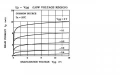
playing around with my HP 339A distortion analyzer again this morning, and settled down to measure the B1 schematic and influence of the transistor types and supply voltages. Here goes:
1KHz, 1Vrms out, matched 9mA Idss
18V+ 2SK170: thd = 0.00105% mostly noise, some H2 and H3 ?
2N3819: thd = 0.01120% pure H3
30V+ 2SK170: thd = 0.00090% mostly noise, some H2 and H3 ?
2N3819: thd = 0.00120% mostly noise, some H2 and H3 ?
unmatched JFETS
Idss 11mA as CCS (lower jfet), drived JFET 9mA: THD = 0.00090%
Idss 9mA as drive jfet, CCS 11mA: THD = 0.00115%
Conclusions:
1] 2N3819 need at least 10V more Vsupply, but then will work very well
2] 2nd harmonic is effectively cancelled, at higher output voltages, 3rd harmonic dominates.
3]it's best to keep the higher Idss JFET as the CCS.
Well it's very effective buffer, with low THD (due to canceling of H2?)..
Cheers,
Thijs
PS
did Nelson make a mistake when he write in Side E "A teensy bit of second harmonic" .. I would think he means 3rd harmonic..
So, if I was to replace Q101 and Q201 with current limiting diodes, what would be the best choice for current? From the 2SK170 data sheet it looks like these draw about 11mA with 9 volts across them? (they don't have 11ma current limiting diodes, only 10mA or 12mA, which do I choose?)
Attachments
Last edited:
Also, if I raised the supply voltage to 20volts, can I replace R2 with a 1mA CCS? This would give a gate voltage of 10volts and it would be much more immune to power supply variance.
- Home
- Amplifiers
- Pass Labs
- B1 Buffer Preamp