using a high-speed comparator AD8561 improves the results by 3-6 dB.
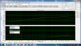
THD 20W 3.9 Ohm 0,0025% 1kHz, and 0,004% 5kHz
THD 20W 3.9 Ohm 0,0025% 1kHz, and 0,004% 5kHz
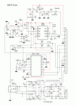

I find some improvements in noise by putting an highest value from resistor to pin3 of IRS20957 (220ohm in my case) with a small value capacitor (47pF) from pin3 to ground.
Thanks, Pergo. I think this is due to the different time of the on / off comparator LM319 (or other with open collector). In my case, the effective rise time is 28ns, fall 8 ns. so I decided to use the AD8561 instead of LM319
I'll try this method, too
I'll try this method, too
Last edited:
In my design i've AD8561 but simpler filter and without RC at the IRS input, output carrier is noisy.
The AD8561 in really really fast. 🙂
An externally hosted image should be here but it was not working when we last tested it.
The AD8561 in really really fast. 🙂
In my design i've AD8561 but simpler filter and without RC at the IRS input, output carrier is noisy.
Perhaps the noise associated with the PCB topology. Or not quite good output inductor. This is the standard UcD? according to my calculations, 1k distortion should be 0.009% @ 7W.
What is the frequency in such a comparator?
The input resistor at IRS was written in a old post in this forum, as a possible solution for bad S/N with high speed oscillation frequency.
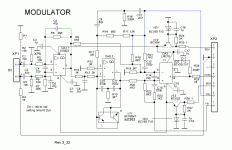
In my case i've 400kHz, but giants mosfets (pair of IRFP4227 + Zetex 9A buffer).
Output inductor is 22uH by Sagami ( http://www.inductor.com/irf/7g31a_e.pdf ).
Amplifier plays without audible noise, with and without that filter.
The 330ohm input resistor to IRS was mandatory.
The 47pF from pin3 to gnd help me improve S/N after some tweaks.
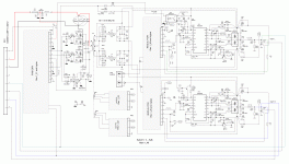
Design was a standard UCD like the Philips AppNote, but with integrated circuits (differential opamp for input buffer + AD8561 + IRS + buffer + mosfet).
Don't know how much was the propagation delay 🙁
In my case i've 400kHz, but giants mosfets (pair of IRFP4227 + Zetex 9A buffer).
Output inductor is 22uH by Sagami ( http://www.inductor.com/irf/7g31a_e.pdf ).
Amplifier plays without audible noise, with and without that filter.
The 330ohm input resistor to IRS was mandatory.
The 47pF from pin3 to gnd help me improve S/N after some tweaks.
Design was a standard UCD like the Philips AppNote, but with integrated circuits (differential opamp for input buffer + AD8561 + IRS + buffer + mosfet).
Don't know how much was the propagation delay 🙁
Faster comparators have higher noise. Generally higher bandwidth means higher noise, since power of white noise is proportional to bandwidth.
Inductor? THD? Whats the connection to noise?
Inductor? THD? Whats the connection to noise?
Good work. This has a lot in common to something I did a few years ago. Reasonably clean.
Output capacitor has inductance, output inductor has capacitance. This introduces one or more zeros in the response of the filter (attenuation ceases past ~1Mhz).
In fact this is good to some point for 2 reasons: Dimensioned properly it can do some "carrier suck-out" and reduce switching frequency drop near clipping and thus distortion. Also, it boosts HF component of feedback signal and allows longer traces from output filter to modulator. But then the boosted HF (and any picked up noise) need to go through one pole to level HF and attenuate picked up noise in the process. This is specially important with fast comparators. The 22pf capacitor from compatarot IN+ to IN- does this job. Slow comparators have a lower pole built-in.
There is one more potential issue: Comparator bounce. The trick is to arrange traces and parasitic capacitances from OUT+ (and OUT- when available) to IN- and IN+ in such a way that there is slightly more HF positive feedback, this results in clean output transients. Too much positive or negative feedback through parasitic capacitances and distortion and noise increase due to inaccuracy.
There is a circuit that can be used to suppress comparator bounce when many channels are put together with a SMPS and environment is noisier than desirable: A zero latency filter. It can be made with a single 74LVC1G0832 gate, two resistors, two capacitors and two diodes. A ZLF detects the rising and falling edges at input and holds output at that level for some time, masking subsequent bounce for some time after first edge. Masking has to be long enough to mask FET switching time, but not long enough to force to be longer the shortest pulse produced by modulator (which is at least two times propagation delay).
Here rise time comparator LM319, fall exactly the same.There is no noise or spikes
Rashly thought that you are talking about the noise level at the output ...
ad8561 looks similar, but is faster
Rashly thought that you are talking about the noise level at the output ...
ad8561 looks similar, but is faster
Attachments

Last edited:
Thanks.Good work. This has a lot in common to something I did a few years ago. Reasonably clean.
have long known that in this case important thing is correct PCB layout.
In my case it would be possible to apply synchronization on the first watts output power to reduce noise for the best THD+N. but in my amp without syncing THD + N near 100 dB@1W😉
Last edited:
The most demanding condition to check for glitches at comparator output is when entering and leaving clipping with substantial current flowing into speaker circuit. If there is no bounce in this condition there won't be when the amplifier is idle, but the opposite is not always true.
In my latest work I'm getting >112dB SNR from 4 channels (+/-70~90V) + SMPS sharing same PCBs (daughter card approach), all without synchronization. Multi-layer PCBs. But this includes limiter and other signal features, this kind of modulator alone can get to 116~120dB SNR easily. During past year I did some research into the techniques to put several channels together. For example, a high DC offset makes SNR worse than a low DC offset. Mismatches in parasitic capacitances (or parts) leading to one channel trying to oscillate at a different idle frequency than another also give worse SNR. When channel matching and DC offset is optimum most of the interference becomes nulled at low output levels because "friendly" synchronization through cross-talk will take place (duty cycles will be nearly the same, and the signal picked up through cross-talk will be just un-distorted audio). As level is increased (dissimilar signals) this weak friendly synchronization is lost, interference becomes distorting in nature. If cross-talk is low enough this will happen at substantial amplitude, when it does not contribute significantly to own channel THD or to audible artifacts.
Glad to see someone caring about details in waveforms. If carrier residual is clean at comparator input, a lot of problems are solved.
Last edited:
I just put this in spice, this seems SUPERIOR design to all what I have seen so far !!!
How you came across this method anyway? This may have even better THD results then "ucd hypex" !! Thd in my spice setup for this is 0,001 % for the same setup compared to 0,1 % for original UCD !!!!
How you came across this method anyway? This may have even better THD results then "ucd hypex" !! Thd in my spice setup for this is 0,001 % for the same setup compared to 0,1 % for original UCD !!!!
I just put this in spice, this seems SUPERIOR design to all what I have seen so far !!!
How you came across this method anyway? This may have even better THD results then "ucd hypex" !! Thd in my spice setup for this is 0,001 % for the same setup compared to 0,1 % for original UCD !!!!
Thanks!
This modulator works well up to 100W.
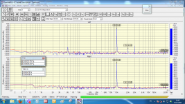
Unfortunately, the real amp shows worse results than 0.001% THD, (see atach.)
At the bottom of the real car amplifier measurements, power - 13 volts.
The load is 3.3 ohms. 15 W 1 kHz, and the sweep of the frequency at 10W
(Worst-channel amplifier, best-DAC-ADC only)
P.S.
You can pay attention to my new design ncore topology amp, somewhere there is a theme. There are the same distortion in the whole range up to 1/2 power THD values do not exceed 0.002%. On 6kHz 50W THD + N of less than 0.0008%.
Attachments
Last edited:
Thanks!
This modulator works well up to 100W.
Unfortunately, the real amp shows worse results than 0.001% THD, (see atach.)
At the bottom of the real car amplifier measurements, power - 13 volts.
The load is 3.3 ohms. 15 W 1 kHz, and the sweep of the frequency at 10W
(Worst-channel amplifier, best-DAC-ADC only)
P.S.
You can pay attention to my new design ncore topology amp, somewhere there is a theme. There are the same distortion in the whole range up to 1/2 power THD values do not exceed 0.002%. On 6kHz 50W THD + N of less than 0.0008%.
I just put this in spice, and it seems to be unstable when output signal is at 75% of Vcc, maybe we can repair this ?! I have seen this method in some paper, can not recall where: But here THD rises as frequency increases but it is always below UCD original. My simulation shows 0,0003% at 200 hz, 0,002 at 1 khz, 0,004 at 3 khz, 0,04 at 10 khz, but it is always better then original UCD.
Can you please link this N core design you made ?
- Home
- Amplifiers
- Class D
- Automotive UcD high-quality power amplifier 2x100W