I believe that Permender used the schematic from the NP article for the CX1:
http://www.firstwatt.com/pdf/art_sony_vfet_pt1.pdf
I have looked at the board carefully, and it looks to be the exact circuit, including the buffer for single ended input.
I have a question for the panel : I am planning a dual mono amp with the PSUs in a separate case. The main PSU will be directly from the VFET article. Permenders boards take the AC from the bias transformer directly. Could I use a bridge rectifier in the PSU case, so as not to pass AC current from PSU to the amp case? Are there suggestions to do this in a working manner. Or is this low voltage AC just not worth stressing over? I have not arranged the cases, nor purchased power connectors.
As a run up to the presentation of part 2, I have posted the original 2013
article Sony VFET 40 Year Commemorative Amplifier
You will find it under articles at FIRST WATT
This is the big brother of the DIY Sony VFET part 2
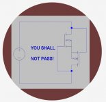
And there is great honor for he who spots the error in the simplified schematic.
A master of the pen, amongst other things naturally. thx


- Status
- Not open for further replies.
- Home
- Amplifiers
- Pass Labs
- Article - Sony VFETs part 1