Hi Frank,
I used the PhaseLink P661-47XC as a simple clock Low Phase Noise Clock Source. PhaseLink don't seem to have the Data sheet on there Web site – If you email me I can send you the PDF – its about 195KB so cannot "post" it on the Forum.
John
I used the PhaseLink P661-47XC as a simple clock Low Phase Noise Clock Source. PhaseLink don't seem to have the Data sheet on there Web site – If you email me I can send you the PDF – its about 195KB so cannot "post" it on the Forum.
John
Class-I
Hi Frank,
Thanks to you guys, for the links.
I don't know, if I understand you right, in my opinion Class-I and the NBDD configuration are the same, NBDD was described here: Karsten Nielsen: A Review and Comparison of Pulse Width Modulation (PWM) methods
for analog and digital input switching power amplifiers
102nd AES Convention, 1997 March 22-25, Munich, Germany, pp.4-6, 34-38.
At least they are very similar, their output is also the same as the TI-version. One can discuss the type of commutation, with or without FET's connected in parallel to the freewheeling diodes (I would say, the additional FETs are better, because of the symmetry). Jaka already posted a very similar configuration in #278/#285. The only difference is the connection of the inductors/transformers. Correct me, if I'm wrong.
I believe, Gyula realised a combination of the Class-I and the Siemens-style converter with the inductors combined to transformers, not the schematic, which he posted, digitalis.zip.
The AES-papers are better for the explanation of the principles.
The important ones are described in Karsten Nielsens Physical degree thesis.
I hope, this will do, especially the drawings.
Also see Circlotrons explanations
Regards, Timo
Hi Timo,
You are correct, class I (or BCA or OCA) and NBDD both use the same modulation scheme. The difference is in the output stage. I posted two links about class I advantages in post#145.
Coupled inductors are also idea of Karsten Nielsen (disregarding the fact that they are known in power conversion industry for more than 20 years). It is also possible to couple inductors in class I design, but with relative loose coupling. Advantage of coupled inductors is elimination of common mode output voltages in full bridge output stages.
Best regards,
Jaka Racman
Hi Timo!
I usually saw the topics, this is really something like fanatism as it's in the logo above. In the circuit, the output stage was modified for the standard bca, the Source-to-Gate stripe had to be cut. The output was coupled to the speakers with a 19000 uF elko.
After the fault I calculated the current flowing across the 47 uH coil paralleled with the MBR at the Gates, and it turned out that the current has very slow rising. Formerly I had to hurry with the circuit (this was my dissertation 😉), and just probed the coil (which I used for the TORX) parallel with the schottky. The result was good on the scope (of course, because the output filter coil's self induction appeared as the switching) and I can't try it with load, the supply hadn't been completed yet. Now I understand why wouldn't it sounds good with the speakrs in class-D, the fets only just caught the conduction. I made the calculations some days ago and find the 47 uH must be somewhere about 1.5-2 uH for the proper deadtime. This is why the BCA wouldn't work at higher supply voltage. The turned over schottky and 47 uH pairs could hardly discharge the Gates and the coils saturated. But it sounded so good!
I think Jaka would make a multi-phase modulator because of the ripple-frequency rising, ripple-amplitude decreasing and to add some null riple points to the signal levels.
I'm worried about Crown patented the topology. It can't be made by anyone else.
Bye,
Gyula
Gyula will be back in 3 months..
I'm worried about Crown patented the topology. It can't be made by anyone else.
Of course it can ! But only for non-commercial purposes.
regards
Charles
Hi,
Crown made a mistake and patented topology only with analog modulators. Cirrus logic just managed to patent the same topology with digital modulators (US 6693571). I wonder what they overlooked this time? Coupled inductor extension maybe?
Best regards,
Jaka Racman
Crown made a mistake and patented topology only with analog modulators. Cirrus logic just managed to patent the same topology with digital modulators (US 6693571). I wonder what they overlooked this time? Coupled inductor extension maybe?
Best regards,
Jaka Racman
So nobody can make circuits for sale with Class-I except Cirrus Logic and Crown? This is a way to put a crimp in everybody' style. What a sass! Is this the same case with Class-D too?
Is this the same case with Class-D too?
The longest run-time for patents is 25 years (differing between countries). Class-D was "invented" along time ago, so basic class-D is public domain. But you can patent certain class-d topologies, what has been done quite intensively.
Regards
Charles
Hi Gyula,
things are not so black and white. First, Cirrus Logic is in the bussines of making chips, and when they sell you the chip they grant you the license for the circuit it is used in. TI TAS modulator chips are also patented.
Second iIf you are clever enough, there is almost always a way around a patent. You must concentrate on patent claims, not description. If something is missing from the claims, then you are okay. There has been a lot said in this forum about patents. Search for "patents on class D".
Best regards,
Jaka Racman
Hi Gyula,
at first I want to wish you a successful completion of your dissertation. Unfortunately I stopped halfway 1994. So do your best! And Thanks for your explanations, which I have to think over a little bit.
That terrible external triggered triangle generator! My simulated suggestion does not seem to be so good in reality. I could not get it DC-stable. Thus I tried John's version, but with an inverting comparator instead of the logic IC (as a 'proof of concept', using a slow OPA TS462 and a LM393, both from STM).
Currently I use an external function generator as the trigger and a grounded scope, maybe, they disturb the signal a bit. There remains a DC-jitter on the triangle, lowering with smaller values of the feedback resistor. But its value should be kept above around 10k, because the fed back rectangle would disturb the reference and interfere with the triangle signal otherwise.
John, did you analyse your circuit? May I expect significantly better results with faster ICs (AD8033 as OPA and MAX942 as Comparator)?
Regards, Timo
Hi Gyula
I didn't follow all the posts before. What do you need your triangle generator for ? Are you building an "ordinary" class-d amp ? What are your linearity requirements for the triangle generator ?
Regards
Charles
I didn't follow all the posts before. What do you need your triangle generator for ? Are you building an "ordinary" class-d amp ? What are your linearity requirements for the triangle generator ?
Regards
Charles
Triangle generator
Hi Charles,
yes, an ordinary Class-D. NBDD-configuration with a 'simple' triangle-to-PWM-conversion. In the end, this amp should incorporate a error correction by feeding back the output (before and hopefully after the output filter) to the inverting input of the input signal amplifier (similar to be seen in the Siemens-paper).
The second university project combines a MSP430-µC with an one-quadrant PWM-heater control (max. 20W, but fast reaction times), which should be synchronised to the µC clock for EMI reasons.
The linearity requirements for the audio amp are significantly higher, if I do not rely on the NFB only. Until now I did not think over the correlation between the triangle linearity and the dsitortion level to be obtained. I also don't know, how to measure the linearity of the triangle unless I would compare the PWM-timing to the input signal. The linearity itself of John's solution seems to be o.k., because of the constancy of the integrating current and therefore the input voltage due to the lack of a coupling capacitor, inside one PWM-cycle.
Regards, Timo
Since you are incorporating an overall feedback loop the linearity problem is a bit relaxed. But you should get quite good resultd by the use of a binary counter (to generate a proper rectangurlar), followed by an ordinary inverting Integrator. To avoid runaway of the Integrator a parallel resistor should be placed to the capacitor. The time-constant of this parallel RC circuit should be larger by one or two orders of magnitude than the Integrator time-constant in order to achieve good linearity. You also need a series cap at the input, which has to be chosen reasonably large as well.
Here you can see what I am talking of:
http://www.diyaudio.com/forums/attachment.php?s=&postid=194684
Regards
Charles
P.S. Regarding your second application: Depending how accurately the heater must be controlled, it would be easily possible to achieve this PWM (or why not delta-sigma) modualtion directly by software.
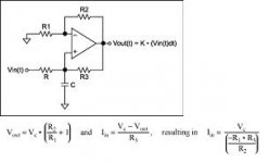
Deboo integrator
Hi,
I’ve built circuits based on the topology shown, it’s very important to get the values correct on the DC FB filter components to prevent the DC stability problems. I also seem to remember I was never able to reduce the resultant “Spurs” offset from the carrier, below –100dB.
A far more elegant solution is to use a Howland current source with a capacitive load, also known as a Deboo integrator.
The Deboo integrator is NON-INVERTING, has both a ground-referenced input and output. Consider the circuit in three parts: the input resistor R, the integrating capacitor C, and the right side of the circuit — which is equivalent to a negative resistor connected to ground.
The input current equals the input voltage divided by a negative resistor. The negative resistor just changes the direction of the input current.
Search the MAXIM Website for more detailed information (Deboo Intergrator) – sorry I don’t know how to post links…
Attachments
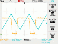
triangle
John and Charles,
Once again, many Thanks for your hints. I will pore over them.
The correction of my triangle try is to be seen in this directory. Read the description file, if interested.
Charles, the software control was realised with a three-level-control (via integrated 12bit ADC and external 12bit DAC) and a cycle of 1ms. This was too slow for our application, therefore I decided to do it in hardware, to free the controller (MSP430F149) from the control business and to achieve much lower cycle times (target 50µs). The SW-PWM with a minimum resolution of 12 bit could achieve a cycle time of 512µs at 8MHz clock, not much better than the current solution.
John, to post links, click on the http-button at the fourth row of the post reply page, you will be prompted for a phrase first and then for the real link - easy.
Regards, Timo
Attachments
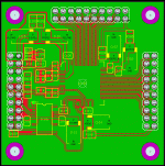
Hi,
Attached is picture of my TAS5076 modulator board. I have decided to use modular approach, so this little board has only TAS5056 and SRC4192 with decoupling capacitors. This little module will sit on a larger motherboard which will contain clock, SPDIF receiver, power supplies, micro controller for TAS5076 control etc.
I intend to experiment on motherboard with various clocks, power supplies etc. As John has pointed out, clock performance is major parameter in achieving good results with digital modulators. So I have decided to route balanced signal (LVDS or PECL) for clock to my module and have balanced to TTL converter on the module.
The problem is, I have no idea what to use for balanced to TTL converter. Clock frequency will be 25MHz, since TAS5076 uses internal PLL. So far I think my possible choices are:
fast comparator like AD8611, LT1719, MAX999, LMV7219,
LVDS receiver like TI SN65LVDS34D, MAX9130, MAX9111
PECL to TTL translator like ON MC100EPT21D.
Comparator would be the most universal possibility since it would allow also unbalanced (sine wave) clock source, but on the other side PECL to TTL translator has 500ps rise and fall times and 0.2ps typical jitter. Because of internal PLL in TAS76 that probably is not a great advantage.
I would really like to have some advice, since I have zero experience with clock sources.
Best regards,
Jaka Racman
Attachments
Jaka,
I used the TI LVDS SN65LVDT20 & SN65LVDS10 SOT23 TX & RX devices on a recent design. I found there Phase Noise performance @ 100MHz to be poor. Despite data sheet claims for sub pS jitter performance, it is not stated how this was measured, over what frequency bandwidth & what form / length of interconnect was used between the devices.
LVDS is EXTREMELY again read !!EXTREMELY!! sensitive to coupling from secondary sources such as Fast edge CMOS signals – even on a well designed / ground plane 4 layer PCB. The LVDS devices I have tried have VERY poor LF noise performance – i.e. close in carrier noise. Maybe both issues are due to the Low Level signalling current used in LVDS technology.
Due to the poor performance of LVDS on the design, I hand modified the PCB to UHS CMOS clock distribution and gained an extra 5dB to 6dB dynamic range.
During the design of the above board, I used a TEK 11801C & SD24 TDR system to optimise the PCB termination components – with very little benefit, so this can be discounted as a source of error.
I also found that the performance of the above LVDS logic quickly fall apart with increasing clock rates – maybe they will work better @ 25MHz, but you would still have the LF issue.
I would VERY strongly recommend that you place your clock oscillator on the modulator PCB, as this is the critical node. Distribute the clock from the XO in two separate buffered paths with Fairchild UHS tiny logic inverters – I use the NC7WZ04P6 Dual inverters – supplying a separate clock path to the modulator and the SRC.
Although the TI has an internal PLL, its still good to know that you have provided it with the best clock you can – I guess no argument here!
To reduce noise on the PCB I would strongly recommend squeezing 27Ohm series termination resistors on all of the PWM outputs. This really helps to reduce ground noise / EMC - Good Luck!!
SRC Again
When feeding the 5015 with fs of 200 kHz from the SRC4192, do you bypass the digital interpolation filter of the 5015, because the signal is already upsampled?
And is this how one can get the advantage of the better stopband att. @ 140db from the SRC?
Frank 😕
When feeding the 5015 with fs of 200 kHz from the SRC4192, do you bypass the digital interpolation filter of the 5015, because the signal is already upsampled?
And is this how one can get the advantage of the better stopband att. @ 140db from the SRC?
Frank 😕
Frank,
Lets say you up-sample with the 4192 to 200KHz from 44.1KHz, you will then gain the 140dB + stop band rejection of 4192 over the 22 to 200KHz BW, the TI’s poorer internal filter will now operate from 100KHz (Fs /2) – luckily well above the audio band.
Lets say you up-sample with the 4192 to 200KHz from 44.1KHz, you will then gain the 140dB + stop band rejection of 4192 over the 22 to 200KHz BW, the TI’s poorer internal filter will now operate from 100KHz (Fs /2) – luckily well above the audio band.
Hi Frank!
The digital interpolation filter of the TAS5015 upsamples the input sample values 8-times at 32, 44,1 and 48 kHz, 4-times at 88,2 and 96 kHz, 2-times at 176,4 and 192 kHz. So the pwm outpull will be at (256) 352,8 - 384 kHz. The upsamler is the most disadvantage of the TAS501x because if it could be bypassed, a feedbacked amplifier could be made with a fast DSP. The DSP could receive the input data and does all of the signal processing what the user want to, then send the the PCM values directly to the Equibit modulator at 384 kHz. A fast two-way ADC could sample the outputs at 384 kHz or faster, and send the values directly back to the DSP. The advantage of this solution is the removed delay caused by the interpolator and the overall short delay. This might be a good amp.
But it isn't realizable with the TAS series.
Regards,
Gyula
- Status
- Not open for further replies.
- Home
- Amplifiers
- Class D
- Anyone interested in a digital amplifier project?