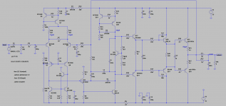
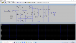
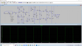
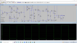
I played with this a bit and here is where I would go with it. I threw in two pole compensation, but the values are just a guestimate. Marcel can probably recommend better choice for C3, C18, R36. I did not include a phase margin probe. 1N4148 are not the ideal diode for Baker clamps but they don't seem to compromise THD here. Rail sticking on this amp is not bad without them so maybe don't bother. Let us know if you don't understand something I did. I replaced the static labels with .op labels that will update when you run the simulation, but I can't find a way to make their font larger.
You may notice that the input THD is now zero. Setting the simulation parameters with .par statements maybe doesn't work.
You may notice that the input THD is now zero. Setting the simulation parameters with .par statements maybe doesn't work.
Attachments
Last edited:
Thank you , very much appreciate it. Can you please include the models of bd140-139 and mpsa.I played with this a bit and here is where I would go with it. I threw in two pole compensation, but the values are just a guestimate. Marcel can probably recommend better choice for C3, C18, R36. I did not include a phase margin probe. 1N4148 are not the ideal diode for Baker clamps but they don't seem to compromise THD here. Rail sticking on this amp is not bad without them so maybe don't bother. Let us know if you don't understand something I did. I replaced the static labels with .op labels that will update when you run the simulation, but I can't find a way to make their font larger.
You may notice that the input THD is now zero. Setting the simulation parameters with .par statements maybe doesn't work.
And if you have time , I have a few questions:
-You replaced the two 100ohm "Degeneration" resistors with one 22ohm between their emitters , now R30 and R11 act as "degeneration resistors" ? why are they so big like 4.7k ? .
-what does R12 with D3 and R6 do?
-C18 , C3 is two pole compensation , isnt it also " inclusive compensation" or whatever its called , with the output trough R36 ?
-C15 in the output transistors bases , helps with on off speed?
- What is / is there any difference of using Q13 Q14 (pre drivers) emitters togheter with a 1k resistor, and the drivers with 100ohm togheter, not connected to the " output rail " compared to using a resistor on each emitter to the output like this:
Attachments


1. I used a single (22 Ohm) resistor so that you can adjust the degeneration with a single resistor. The 4.7K resistors are a large value, in series with the current source that drop a small voltage but have little effect on the resistance between emitters. I reduced the degeneration to increase the feedback and improve distortion, but I did not check the phase margin, so it probably needs adjusting.Thank you , very much appreciate it. Can you please include the models of bd140-139 and mpsa.
And if you have time , I have a few questions:
-You replaced the two 100ohm "Degeneration" resistors with one 22ohm between their emitters , now R30 and R11 act as "degeneration resistors" ? why are they so big like 4.7k ? .
-what does R12 with D3 and R6 do?
-C18 , C3 is two pole compensation , isnt it also " inclusive compensation" or whatever its called , with the output trough R36 ?
-C15 in the output transistors bases , helps with on off speed?
- What is / is there any difference of using Q13 Q14 (pre drivers) emitters togheter with a 1k resistor, and the drivers with 100ohm togheter, not connected to the " output rail " compared to using a resistor on each emitter to the output like this:
2. R12, D3, C7 do two things. First, they filter the supply ripple and slump. Second, they hold the LTP up for a short time during power down to reduce thumps. R6 filters the supply noise for the VAS, so that the compensation current returns through C8 and not so much through the power supply. Bruno Putzeys has a AES paper about this problem but this is a simple compromise solution.
3. I don't care what it's called, and I'm not a compensation expert. If I spent more time on it, I would fiddle with the phase margin plot until it looks good.
4. Yes, it helps reduce shoot through conduction when driven by high frequencies and improves THD.
5. This is cross coupling so that as much of the opposite driver output is available to drive the next stage off as is practical. It improves crossover distortion because the driver current must go to one or the other following bases and none is wasted in resistors. There is less/no time spend when neither of following transistors is driven.
All these things are open to discussion, and I expect other opinions, but most of this is standard practice. For example, many people think a "non-switching" output is the best idea. Being very concerned with reliability and efficiency, and pragmatic about THD, I'm not a "non-switching" fan. Amplifiers that feature PPM THD are usually unreliable, inefficient and unstable.
PS, I will attach my models for MPSA06/56 and BD139/140, but these are common devices and spice models are available from Onsemi etc. You might use 2N5550 and 2N5401 instead.
Attachments
Last edited:
IanHegglun has a thread on the subject.
https://www.diyaudio.com/community/...and-non-switching-auto-bias-power-amp.375141/
It's about class AB crossover distortion.
https://www.diyaudio.com/community/...and-non-switching-auto-bias-power-amp.375141/
It's about class AB crossover distortion.
I know that thread, but didn't realize Ian was aiming for ppm distortion levels.
I have had a non-switching amplifier with a class-AB bias loop (autobias) since I designed and built one in 1994, its THD is about 25 ppm at 10 kHz at half power, 60 ppm at 80 % of maximum power. My target was anything below 100 ppm.
There were two reasons for using a class AB bias loop: I wanted to be sure that the distortion would be independent of temperature changes of the output devices and I just find it more elegant than the usual methods. With an AB loop, making it non-switching is a matter of choosing the right non-linear function for the loop.
Anyway, it's off topic.
Thank you very much !. So with the asc. with the modifications you posted it simulates Total Harmonic Distortion: 0.000241%,1. I used a single (22 Ohm) resistor so that you can adjust the degeneration with a single resistor. The 4.7K resistors are a large value, in series with the current source that drop a small voltage but have little effect on the resistance between emitters. I reduced the degeneration to increase the feedback and improve distortion, but I did not check the phase margin, so it probably needs adjusting.
2. R12, D3, C7 do two things. First, they filter the supply ripple and slump. Second, they hold the LTP up for a short time during power down to reduce thumps. R6 filters the supply noise for the VAS, so that the compensation current returns through C8 and not so much through the power supply. Bruno Putzeys has a AES paper about this problem but this is a simple compromise solution.
3. I don't care what it's called, and I'm not a compensation expert. If I spent more time on it, I would fiddle with the phase margin plot until it looks good.
4. Yes, it helps reduce shoot through conduction when driven by high frequencies and improves THD.
5. This is cross coupling so that as much of the opposite driver output is available to drive the next stage off as is practical. It improves crossover distortion because the driver current must go to one or the other following bases and none is wasted in resistors. There is less/no time spend when neither of following transistors is driven.
All these things are open to discussion, and I expect other opinions, but most of this is standard practice. For example, many people think a "non-switching" output is the best idea. Being very concerned with reliability and efficiency, and pragmatic about THD, I'm not a "non-switching" fan. Amplifiers that feature PPM THD are usually unreliable, inefficient and unstable.
PS, I will attach my models for MPSA06/56 and BD139/140, but these are common devices and spice models are available from Onsemi etc. You might use 2N5550 and 2N5401 instead.
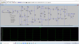
So, here is the current schematic, if anyone has any more ideeas, maybe some help with the values of C3, C18, R36 ,
it simulates Total Harmonic Distortion: 0.000241%, if that is accurate .
Thank you everyone for taking a bit of time to reply and help. Im sorry I didnt post, reply so often, with work Im not that active on my pc lately.
@steveu "
played with this a bit and here is where I would go with it. I threw in two pole compensation, but the values are just a guestimate. Marcel can probably recommend better choice for C3, C18, R36. I did not include a phase margin probe. 1N4148 are not the ideal diode for Baker clamps but they don't seem to compromise THD here. Rail sticking on this amp is not bad without them so maybe don't bother. Let us know if you don't understand something I did. I replaced the static labels with .op labels that will update when you run the simulation, but I can't find a way to make their font larger.
You may notice that the input THD is now zero. Setting the simulation parameters with .par statements maybe doesn't work. "
@MarcelvdG Should I still use a cap from Q7 to negative rail , I should test again what you suggested with the ringing.
@Mooly If you'd like to take a look.
Attachments
No one , but I certainly will do. I will post here .how many people have build this amp?
It's a pity, the amplifier sounds exactly like adjusting the frequency compensation.3. I don't care what it's called, and I'm not a compensation expert. If I spent more time on it, I would fiddle with the phase margin plot until it looks good.
Selecting the necessary operating currents and topology is easy and not always decisive.
Turn off C1 at the input and apply a meander - this circuit should keep the amplifier in a stable state, i.e. the meander at the output must be free of emissions, you can also additionally check with a 1 kHz sine wave at the maximum input amplitude voltage.So, here is the current schematic, if anyone has any more ideeas, maybe some help with the values of C3, C18, R36 ,
@MarcelvdG Should I still use a cap from Q7 to negative rail , I should test again what you suggested with the ringing.
I would be in favour of that, others may have a different opinion.
Thinking about this some more:
1. You maybe should consider output protection. VI limiting has stability issues, but it should have a current limit so that it will survive a momentary short. Given a 35V supply and a minimum load of 4 Ohms, a limit under 10Amps would be appropriate. Using the 0.1 Ohms emitter resistors, you need to divide the Re voltage about 65% for a 0.65V Vbe current sense. That gives you a bit of margin.
2. 10mA VAS current is probably enough for a 2EF outputs (~=10A/30/30). For 3EF, 13mA is more than enough, but it becomes a matter of speed and distortion. I would probably fall back to about 5mA and then you could use smaller faster transistors.
Antiparallel diodes (1N4148 or so) across the base-emitter junctions of the input transistors will also make it more robust, but then against excessive input levels.
do you finish it now?No one , but I certainly will do. I will post here .
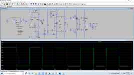
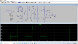
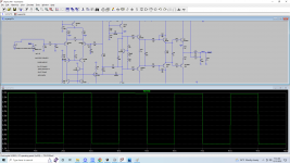
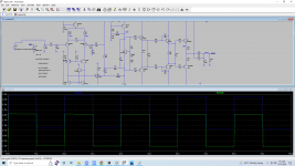
It seems the output waveform is not symmetrical, I only get the positive cycle. maybe I made a dummy mistake or is something else wrong.It's a pity, the amplifier sounds exactly like adjusting the frequency compensation.
Selecting the necessary operating currents and topology is easy and not always decisive.
Turn off C1 at the input and apply a meander - this circuit should keep the amplifier in a stable state, i.e. the meander at the output must be free of emissions, you can also additionally check with a 1 kHz sine wave at the maximum input amplitude voltage.
Attachments
-
 both output transistors.png60.7 KB · Views: 62
 -
 VAS current.png62.1 KB · Views: 60
 -
 pre driver + rail current.png61.9 KB · Views: 60
 -
 pre driver - rail current.png60.5 KB · Views: 59
 -
 driver +rail current.png60.6 KB · Views: 56
 -
 driver -rail current.png61.4 KB · Views: 65
 -
 output transistor +rail current.png59.1 KB · Views: 59
 -
 output transistor -rail current.png60.5 KB · Views: 55
 -
 output transistor -.png61.6 KB · Views: 54
 -
 output transistor +.png61.6 KB · Views: 53
 -
 input.png64 KB · Views: 57
 -
 Output.png63.7 KB · Views: 51
 -
 Vas.png62.1 KB · Views: 49
 -
 pre driver +.png60 KB · Views: 47
 -
 pre driver -.png61.5 KB · Views: 47
 -
 both predrivers.png61.1 KB · Views: 52
 -
 driver+.png60 KB · Views: 52
 -
 driver-.png61.6 KB · Views: 62
It seems the output waveform is not symmetrical, I only get the positive cycle. maybe I made a dummy mistake or is something else wrong.
Attachments

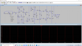
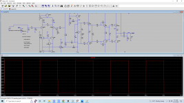
If i do only pulse, one way + or - it does it.It seems the output waveform is not symmetrical, I only get the positive cycle. maybe I made a dummy mistake or is something else wrong.
Attachments
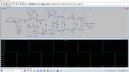
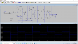
Seems to work fine now if I remove C5 for some reason.It seems the output waveform is not symmetrical, I only get the positive cycle. maybe I made a dummy mistake or is something else wrong.
Attachments
- Home
- Amplifiers
- Solid State
- Any thoughts about this?