Yes , thank you for repying, Im not quite sure how to check for ringing, if you could please explain. and for the zobel newtork I'll use what you suggested.See post #15.
would it benefit to have the capacitor there even if it does not ring?.See post #15.
I'm not a supporter for the arrangement of Q2, leds D1 & D2 and R8 to fashion the cascode base voltage.thank you!. I will add that. any other ideeas? do you think the amp will work fine the way it is in post 1 . ?
Supply noise can inject through R8.
Q2 has two functions: supplying current for the cascode bias and for the differential. I prefer to split these functions.
The negative rail can be isolated then.
Can you suggest a way of biasing the bases of the cascode ?.I'm not a supporter for the arrangement of Q2, leds D1 & D2 and R8 to fashion the cascode base voltage.
Supply noise can inject through R8.
Q2 has two functions: supplying current for the cascode bias and for the differential. I prefer to split these functions.
The negative rail can be isolated then.
Yes , thank you for repying, Im not quite sure how to check for ringing, if you could please explain. and for the zobel newtork I'll use what you suggested.
Reduce the amplitude of Vin to 0
Connect a current source from the negative rail to the base of Q7/collector of Q9 and specify that it has to produce a pulse waveform that goes from 0 to 100 uA in 100 ps. (Any value that is at least a factor of ten below the bias current of Q9 and any very short rise time will do.)
Run a transient analysis over 1 us or so and check the waveform of the voltage at the base of Q7.
Don't change the circuit if the waveform goes monotonically to its final value, or first has some overshoot and then monotonically drops to its final value. If it rings, connect a 10 pF capacitor from the base of Q7 to the negative rail to see if that helps. Adjust the capacitance until you have enough to get rid of the ringing, but not much more than that.
There is no serious signal present between R2-R3. Pointless to use it as a voltage reference for the cascodes.Can you suggest a way of biasing the bases of the cascode ?.
Make a separate current source like Q1-Q2 from the negative rail, connect the cascode bases Q5-Q6 and the cathode of D2 and a bypass cap to it and the anode of D1 to ground. That will suffice.
This thread was started only 2 days ago and as post #1 says it's only "built in the simulator", so what do you think?how many people have build this amp?
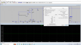
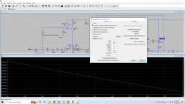
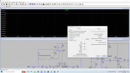
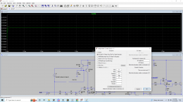
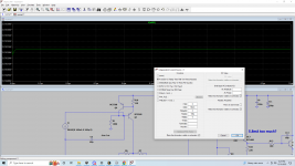
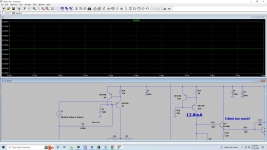
Here are some simulations, I hope I did exactly what you said. Depending on the simulation time, at 1us I didnt get anything, at 10us I think thats the ringing you told me about, 33p is the smallest value at which the ringing is gone.Reduce the amplitude of Vin to 0
Connect a current source from the negative rail to the base of Q7/collector of Q9 and specify that it has to produce a pulse waveform that goes from 0 to 100 uA in 100 ps. (Any value that is at least a factor of ten below the bias current of Q9 and any very short rise time will do.)
Run a transient analysis over 1 us or so and check the waveform of the voltage at the base of Q7.
Don't change the circuit if the waveform goes monotonically to its final value, or first has some overshoot and then monotonically drops to its final value. If it rings, connect a 10 pF capacitor from the base of Q7 to the negative rail to see if that helps. Adjust the capacitance until you have enough to get rid of the ringing, but not much more than that.
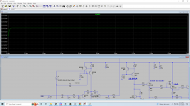
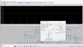
Please take a look, I made a few screenshots with different time periods.
Attachments
-
 1.png64.3 KB · Views: 85
 -
 1us current source 10us sim no cap.png66.9 KB · Views: 71
 -
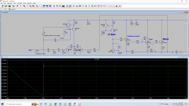
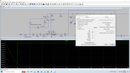 1us current source 10us sim W cap.png66.1 KB · Views: 60
 -
 2.png66.7 KB · Views: 65
 -
 3.png65.3 KB · Views: 63
 -
 4.png67.4 KB · Views: 63
 -
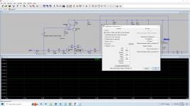
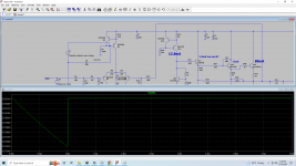
 5us sim 10p cap.png58.5 KB · Views: 61
 -
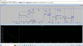
 5us sim 68p cap.png58.5 KB · Views: 64
 -
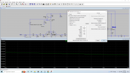
 5us sim.png57.6 KB · Views: 68
Trise was intended to be 100 ps, rather than 1 us or even longer. The pulse width Ton can either be left open or be set to some value greater than the simulation end time.
like this ?Trise was intended to be 100 ps, rather than 1 us or even longer. The pulse width Ton can either be left open or be set to some value greater than the simulation end time.
Attachments

This is how it should look without " ringing" ?Trise was intended to be 100 ps, rather than 1 us or even longer. The pulse width Ton can either be left open or be set to some value greater than the simulation end time.
Attachments
My bad , I dont know how to delete posts, forgot to change TonTrise was intended to be 100 ps, rather than 1 us or even longer. The pulse width Ton can either be left open or be set to some value greater than the simulation end time.
Attachments
ok, and is this fixed ? or it has to be a straight line , like in the second image here.Yes, like post #34.
And this "ringing " is oscillations? is it happening to other transistors in this schematic or , why did you ask only for - Q7 if it's ringing and not other transistors.
Attachments
Like Marcel, I notice the issues with the Darlington VAS and current sources. Unfortunately, the reference designators do not match between the SPICE file and the jpeg, so his comments are confusing if you are looking at LTC spice. To repeat those: the current sources need a cap or a base resistor to guarantee stability. And the first transistor in the VAS Darlington has no current limit, so it will go nuts on the negative clipping; could blow-up. A collector (~1k) resistor that limits to about 30mA is my favorite solution.
But a related possibility is a Baker clamp, and another on the VAS current source. You want to look at rail sticking.
My preference is strictly cross-coupled EFs, ie one resistor (and/or diode) and maybe a "speed-up cap" between driver emitters.
Base stoppers may be useful, and maybe not. I guess you can always short them out.
+/-35VDC exceeds the Vceo of BC456, which is risky, and BD135/136 should be BD139/140 for the same reason.
The VBE multiplier should be by-passed.

Thanks for pointing that out, steveu! I never looked at the .asc files, just at this schematic from the opening post:

I hadn't a clue that there was a version of the schematic with totally different reference designators. So all my comments:
"I would check the response to a small current step of the loop Q7-Q9 to see if it rings. If it does, a small capacitor from the base of Q7 to the negative rail, with or without a small series resistor, could fix that.
A decoupling capacitor across the VBE-multiplier could ensure it doesn't affect the stability of the overall loop.
A small change in the output filter could change it into a first-order series filter, as recommended by A. N. Thiele to reduce the sensitivity to RF signals picked up by the cable to the loudspeaker.
R31 = 8.2 ohm
R32 = 0 (short)
C13 = 33 nF
If you haven't done so yet, check start up, what happens during clipping and during recovery from clipping.
The current through Q13 will probably increase enormously during clipping to the negative rail. You could connect a resistor between its collector and ground with a small decoupling capacitor to the negative rail to keep it from going up in smoke."
are with reference to this schematic!
And the same holds for:
"Reduce the amplitude of Vin to 0
Connect a current source from the negative rail to the base of Q7/collector of Q9 and specify that it has to produce a pulse waveform that goes from 0 to 100 uA in 100 ps. (Any value that is at least a factor of ten below the bias current of Q9 and any very short rise time will do.)
Run a transient analysis over 1 us or so and check the waveform of the voltage at the base of Q7.
Don't change the circuit if the waveform goes monotonically to its final value, or first has some overshoot and then monotonically drops to its final value. If it rings, connect a 10 pF capacitor from the base of Q7 to the negative rail to see if that helps. Adjust the capacitance until you have enough to get rid of the ringing, but not much more than that."
The reason why I asked about Q7-Q9 is that it is a local loop that can easily be poorly damped that is embedded in the overall loop. That can complicate getting the overall loop stable.
I personally would also look at other local loops, like Q1-Q2 and Q10-Q11, and compensate them with a small capacitor or an RC circuit if they ring, but that may be exaggerated, as they are not part of the overall loop and are very unlikely to get unstable by themselves.
By the way, how did you check overall stability?
Last edited:
- Home
- Amplifiers
- Solid State
- Any thoughts about this?